Lecture
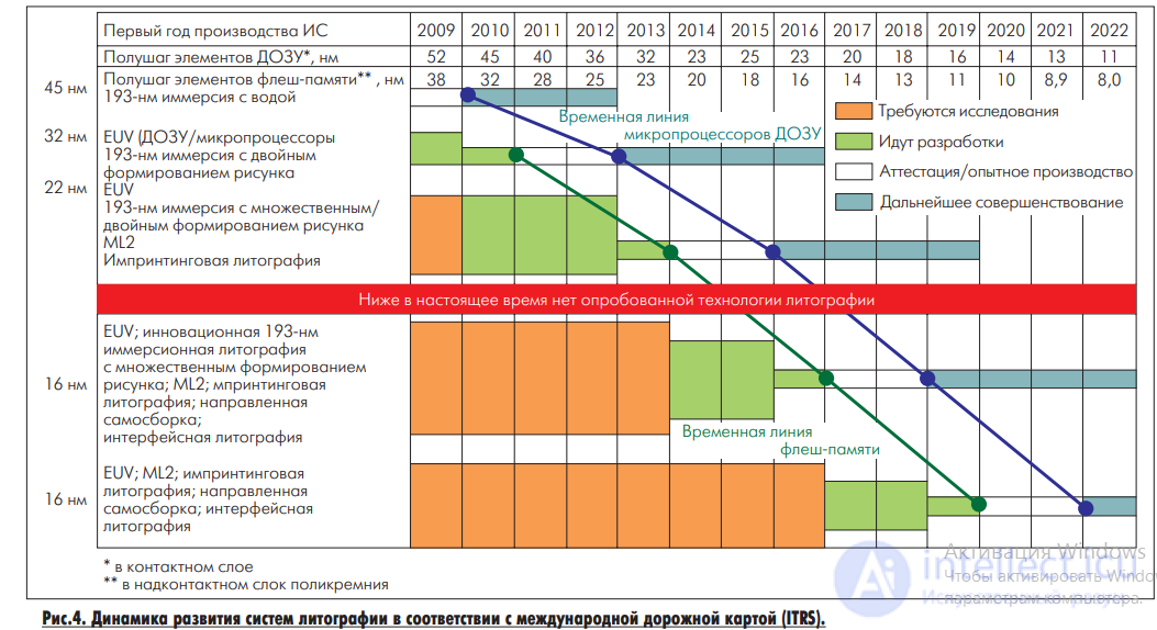
More than once, researchers and analysts predicted that in the coming years the process of miniaturization of microchips will reach physical limits that can no longer be overcome. However, this has not happened yet. The highest degree of integration allows increasing the capacity of microprocessors from year to year and releasing memory crystals capable of storing billions of bits of data. Thus, according to the network development schedule of the industry, approved by the SIA (Semiconductor Industry Association) semiconductor industry association, in 2002 the standard design standards should be 0.13 microns, in 2005 - 0.1 microns, in 2008 - 0, 07 microns and in 2014 - 0.035 microns. The latest figures, in particular, mean that the production of terabit chips on one square centimeter will be located up to 390 million transistors.
However, in addition to purely physical problems, the process of reducing the size of transistors and increasing the degree of their integration already comes up against limitations associated with the characteristics of the production of microcircuits. Generally speaking, the properties of devices that are created on a single silicon wafer, as well as on different wafers, are not identical. Deviations may occur at each of the stages of production. The nature of the likely differences between the crystals produced and the frequency of occurrence of simply defective devices can be a real obstacle to the further miniaturization of the elements of the integrated circuit. Note that miniaturization concerns not only the length and width of the circuit element, but also the thickness of the crystal itself. Transistors and connections on it are realized with the help of a series of levels, in modern chips there may be five or six. Reducing the size of transistors and increasing the density of their placement on the crystal entails an increase in the number of levels. However, the more layers in the scheme, the more carefully must be control over them in the production process, since each of the levels will be affected by the underlying. The cost of improving controls and creating connections between multiple levels can be a deterrent to the increase in the number of layers.
Among other things, the complication of integrated circuits requires the improvement of production conditions, to which, and so, unprecedented high demands are made. More precise mechanical control over the positioning of the original silicon wafer is required. The sterile room (the so-called clean room), where the microchips are created, should become even clearer, in order to exclude the ingress of the smallest particles of dust, capable of destroying the most complicated scheme.
Cost and technology issues in the semiconductor industry are closely interrelated. For the development of modern microelectronics technology and the creation of new industries, huge investments are needed to acquire special technological equipment and to build clean rooms. The complexity and cost of semiconductor manufacturing is constantly increasing. The highest share in the cost of a semiconductor factory is technological and control and measuring equipment. By some estimates, the percentage of this equipment in the total value of the enterprise can reach 50-70%. It is believed that in order to increase production, semiconductor companies need to allocate more than 20% of their annual income for capital needs, and less money is enough to maintain it. For example, Sony announced that it is planning to invest more than $ 880 million in semiconductor manufacturing this year. IBM also announced large-scale plans to expand its semiconductor manufacturing. For this purpose, it intends to allocate $ 5 billion. Moreover, half of this amount will be used to build a modern plant in East Fishkill, which will use all the latest achievements in the field of semiconductor manufacturing, including copper interconnect technology, SOI and high-efficiency insulator technology. The launch of the new plant is scheduled for the second half of 2002, and it will be launched at full capacity in early 2003.
Intel announced that in the current year it plans to invest about 6.8 billion dollars in semiconductor production, which is almost twice as much as last year’s investment, which amounted to 3.4 billion dollars. The company intends to invest 2 billion dollars. to expand its production in Rio Rancho (pc. new mexico). Existing production areas should be increased by more than 90 thousand square meters. m, including over 12 thousand square meters. m reserved for a clean room. The expansion is associated with the transition to a new technological process in compliance with the design standards of 0.13 μm for the manufacture of microprocessors on 300-mm substrates.
Lithography technology
Today, the process of manufacturing chips includes several technological steps, including: lithography, ion implantation, diffusion and oxidation, precipitation, etching, cleaning, planarization and measurement. The most important scientific and engineering developments are carried out in the direction of improving the key stage of the production of an integrated circuit - lithography, since it is here that it is actually possible to reach a certain limit in the foreseeable future. According to experts, lithography has completely exhausted its capabilities by 2003.
The development of lithographic technology from the time of its invention in the early 70s went in the direction of reducing the length of the light wave. This allowed to reduce the size of the elements of the integrated circuit. Since the mid-1980s, ultraviolet radiation produced by a laser has been used in photolithography. In order to put a drawing of the scheme on a plate, photolithography is performed using a computer-controlled machine (stepper). Its purpose is to create in the layer of photoresist material a “window” of a given configuration for the etchant to access the semiconductor plate with an oxide film located below this layer. Such "windows" are formed when a photoresist is exposed in a laser ultraviolet radiation flux; as a result, the photoresist loses (or acquires) solubility. The configuration of the "windows" set the appropriate mask, after applying which the resulting image is condensed using a special lens system.
It is this one that reduces the pattern specified on the mask to the microscopic size of the scheme. The silicon plate is fixed on the position table under the lens system and is moved with its help in such a way that all microprocessors placed on the plate are sequentially processed. Ultraviolet rays from the laser pass through the free spaces on the mask. Under their action, the photosensitive layer in the appropriate places of the plate acquires the ability to dissolve and then is removed with organic solvents. A modern photolithographic machine processes several dozen eight-inch semiconductor wafers in one hour.
Now, most crystals are made using ultraviolet rays with a wavelength of 0.248 microns. To create a number of crystals developed lithographic technology, providing a wavelength of 0.193 microns. However, when photolithography crossed the 0.2 µm limit, serious problems arose that, for the first time in the history of this technology, questioned the possibility of its further use. For example, at a wavelength of less than 0.2 μm, too much light is absorbed by the photosensitive layer, so the process of transferring the pattern of the circuit to the processor becomes more complicated and slower. Such problems encourage researchers and manufacturers to look for alternatives to traditional lithographic technology. For example, the possibility of replacing ultraviolet rays with X-rays has been studied in US scientific laboratories for more than two decades.
Output found
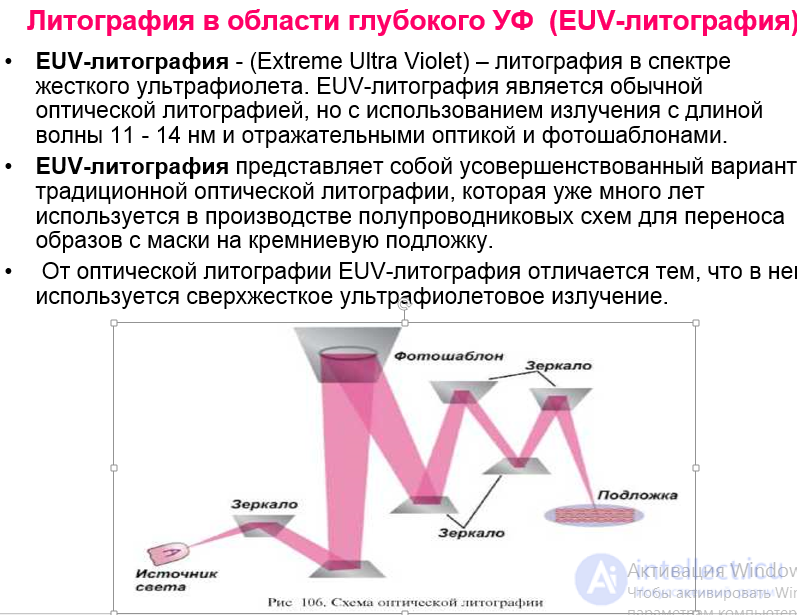
One of the technologies, called EUV (Extreme Ultra Violet) and bringing together several well-known companies, is aimed at improving the process of photolithography in the manufacture of microchips. It is expected that the clock frequency of the processors, which will be manufactured using the new technology, will reach 10 GHz in 2005-2006.
In 1996, Intel began funding research on EUV, and in 1997, together with Motorola and AMD, organized a consortium of EUV LLC (Limited Liability Company). Micron Technology and Infineon Technologies joined this consortium in early 2000, and IBM only in 2001. The rapid progress of the EUV LLC program attracted industry interest and provided it with widespread support.
In the spring of this year, representatives of the computer industry and government structures of the United States announced the completion of work on a prototype of the first plant for the production of crystals using EUV. The laboratories belonging to the US Department of Energy and the EUV LLC consortium worked together to create an experimental test bench (Engineering Test Stand, ETS). In addition, three national laboratories - them. Lawrence Berkeley (Lawrence Berkeley National Laboratory), im. Lawrence Livermore (Lawrence Livermore National Laboratory) and Sandia National Laboratories - joined forces to work on the EUV as part of the Virtual National Laboratory.
As already noted, modern installations for step-by-step replication on a plate using deep ultraviolet radiation (Deep Ultra Violet, DUV) - machines that print circuits on silicon substrates use light sources with a wavelength of 248 nm. The wavelength of the EUV radiation is about 13 nm, i.e., about 20 times smaller. The transition from DUV to EUV lithography provides a more than 10-fold reduction in wavelength and a transition to a range where it is comparable to the size of only a few dozen atoms. The currently used lithographic technology makes it possible to apply a pattern with a minimum conductor width of 0.1 μm, while EUV lithography makes it possible to print lines of much smaller width — up to 0.03 μm. Controlling ultrashort radiation is not as easy as it sounds. Since EUV radiation is well absorbed by glass, the new technology involves the use of a series of four special convex mirrors that reduce and focus the image obtained after applying the mask. Each such mirror contains 80 individual metal layers with a thickness of about 12 atoms.
Over the next year, partners of the EUVLCC consortium and suppliers of lithographic systems will be working at the ETS stand to improve the technology and prepare it for the creation of a prototype industrial plant that meets the requirements of the industry for high-volume production.
To make EUV technology available for widespread use, much remains to be improved in it. In particular, it is necessary to develop a mechanism capable of capturing invisible light, create platforms for combining pictures at various stages of manufacturing the microcircuit, a system of mirrors and defect-free masks, as well as new means of control and measurement.

Comments
To leave a comment
Design and engineering of electronic equipment
Terms: Design and engineering of electronic equipment