Lecture

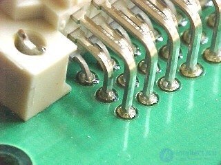
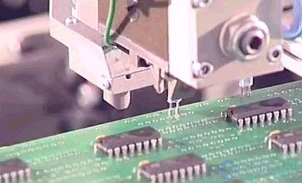
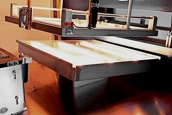
The site of the module mounted on the terminal mounting technology.
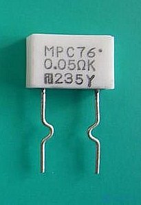
Components installed on the board for option I, without a gap.
The assembly of an electronic module by installing components with leads into holes in a printed circuit board and subsequent soldering is called a lead-in assembly. This type of installation is the progenitor of modern technologies for the production of electronic modules. Output mounting appeared simultaneously with the printed circuit boards. The appearance of the assembly with the use of printed circuit boards in the future allowed to automate the design and manufacture of electronics. Now lead mounting fades into the background, retreating before mounting planar components, but the categories of electronic devices remain where lead mounting dominates other technologies. These are power electronics, power supplies, high-voltage modules and others.
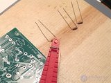
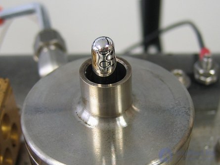
Connector mounted on the board.
There are components that have no analogues in planar design - connectors, relays, transformers for which the assembly can be performed only with the use of terminal installation technology.
Preparation of components for installation is needed to align the flexible terminals of the components. Forming is performed in such a way that the distance between the ends of the component leads corresponds to its installation location on the board and the required distance between the board and the component is ensured. The form of the output components depends on the installation option.
 |
 |
 |
 |
Component leads are molded and installed on the board.
The forming of flexible leads should not damage them, break the coating of the leads, bending is unacceptable at the point of connection of the lead with the body and is performed only at a distance not less than the allowable one. The method of forming should exclude rotation of the output relative to the body of the component. The safety of the glass insulators between the terminal and the metal body of the component must be ensured.
The simple limitations of two sizes, R and L, describe the allowable shape of the bending of the component inference that occurs during molding. The radius R of the bend of the pin depends on the diameter of the pin and is at least two of the diameter of the pin. The smallest gap between the point of entry of the output into the component housing to the vertical axis of the molded output L is in the range of 1 ... 4 mm and depends on the type of the component housing. After forming on the findings should not appear deformation and refinement. Compliance with these simple rules contributes to the safety of components and the reliability of electronic modules.
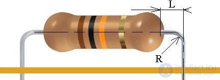
The dimensions of the molded component pin in an enclosure with axial leads.
The component is installed as per option II, with a gap between the component body and the printed circuit board.
The length of the lead from the component body to the soldering area must exceed 2.5 mm. It is forbidden to mold the hard leads of high-power transistors, diodes of medium and high power. It is forbidden to mold the leads of components in housings with many leads, for example, microcircuits in a DIP package.
 |
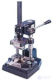 |
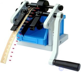
Manual molding equipment.
The molding operation is carried out on manual devices and semi-automatic installations. Molding semi-automatic can perform straightening, stripping and trimming conclusions. Semiautomatic devices can control the electrical parameters of components, produce stacking components in process cassettes.
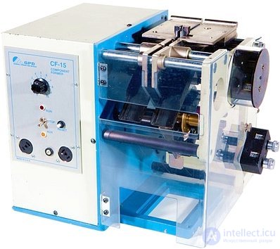
Forming machine.
Components are fed into the molding machine from special tapes, tubular cassettes or placers. The required lead sizes are adjustable, the molding machines are equipped with various molding dies. The design of the molding molds ensures proper molding. For molding equipment, there are automatic counters of components fed from the belt. Productivity of automatic counters up to 360,000 pieces per hour.
Productivity of the automatic molding device:
|
Type of shell |
Axial conclusions |
Radial pins |
|
Of tapes |
40,000 |
20,000 |
|
From placer |
7,000 |
3000 |
Manual feeding of components provides typical molding capacity of about 1,500 ... 3,000 components per hour.
Installation options for lead components on the PCB.
Option I - there is no gap between the component case and the board. This option is well suited for installing components on a one-way board. The conductive pattern is located on the opposite side from the components, which excludes the contact of the component body and the conductive pattern. Reducing the length of the component terminals reduces susceptibility to electromagnetic interference and reduces the emission of self-interference to the air. Components withstand vibration well. The height of the module is reduced. Improved component cooling due to heat transfer to the board, which improves reliability. The disadvantage of this installation option is the difficulty of washing the module from the flux, ensuring the isolation of the component from the conductive pattern in the case of a double-sided board.
Pin forming, providing clearance between the board and the component case.
Option II - between the board and the component housing the gap. Used for double-sided boards. This method of installation helps to remove excess flux by washing, and the heating of the microcircuits during soldering is reduced. Damage to the pads on a one-sided board with a load on the component from the top.
Option III - vertical installation. Components with axial outputs are more dense. This option reduces the manufacturability, increases the likelihood of a circuit between the terminals, increases the height of the module. When installing components vertically, the angle of inclination of the component relative to the vertical axis should not exceed 15 °.
Installing the components should make it easier to read the markings. It is especially important to consider reading the markings of polarity. Maximum ease of marking reading facilitates assembly control.
The assembly of electronic modules using output components can be done manually or with the help of special automatic equipment.
The quality of soldering of the lead component depends on the gap between the lead of the component and the walls of the metallized hole. The gap should provide capillarity, which facilitates the soldering in the cavity between the outlet and the walls of the hole and to ensure the penetration of the flux, the output of gases during soldering. The optimum gap is from 0.3 to 0.4 mm when using lead solders and 0.5 mm when using lead-free solders for boards with a thickness of 1 to 3 mm with holes with a diameter of 0.6 to 1.2 mm.
Manual terminal installation of modules is advisable to use in the following cases: the use of automatic equipment is unprofitable due to the small volume of the order or the assembly of several prototype modules of modules; the boards are not suitable for automated installation, during final installation of terminal elements after automatic installation. Today, electronics is at the level of development not allowing to completely abandon manual installation operations. The installer carefully checks the appearance of each component before installation. If necessary, cleaning the leads from oxides and tinning the leads is performed. It is possible to give the conclusions of each component, the form of the most optimal for installation on the board, due to the design of the electronic module. Manual molding allows you to shape the pins of the components, making it easier to read the markings.

Manual installation.
Some recommendations for manual soldering . When installing, use a soldering iron with a pre-tinned sting. Depending on the mass of the component and the width of the track, it may take from a split second to two seconds to warm up the soldering area. When using tubular and solders in the form of wire soldering is carried out with two hands. For best results, follow these steps. To preheat the surfaces to be joined, simultaneously touch the soldering pad of the card's contact area and the component output. Solder, located on the soldering iron tip, applied when the tip is tinned, contributes to heat transfer due to the larger area of contact between the tip and the soldering area.
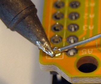
Soldering a soldering iron with two hands.
A solder tube with a flux brought to the soldering area will allow transferring the melting solder to the soldering area. This will take about half a second. If solder is applied to the sting, the flux will burn out prematurely. Remove the solder tube from the soldered joint, and then remove the soldering iron. The entire operation should take from half to two seconds, depending on the soldering iron parameters and the wettability of the soldered surfaces. An increase in the operation time and an increase in the temperature of the soldering iron can lead to an increase in the flux residues; soldering can turn out to be brittle. After soldering, pruning is performed.

Trimming component leads after manual soldering.
Automatic assembly is performed using two types of special equipment: component installers and soldering machines. The advantages of automatic mounting boards: reliability, cost reduction, high accuracy, speed, installation of miniature elements, automatic control. Automatic machines allow for the adjustment of production lines through programming. The quality of automatic installation, as well as its cost, in the application of automated devices is largely ensured at the design stage. Modern technologies allow components with a minimum distance from each other, to fractions of a millimeter, but this is not always justified. Short distances make it difficult to repair, as well as control components and solder joints. Installation of components is carried out with the use of special mounting machines, which also carry out trimming, hemming on the reverse side of the board.
The assembly head of the machine places the component in a radial housing.
Outlet installers are equipped with a set of assembly heads. In most machines, the heads have mechanical grips controlled by a servo drive. The standard angles of rotation of the component are multiples of 90 °. There is a possibility of equipping the machine with an assembly head with a free angle of rotation. A number of machines has the ability to install wire jumpers on the board, cutting them just before installation. Passport performance of modern installation equipment reaches 20000 ... 40000 components per hour. The performance of the installer when installing components of complex shape can be less than ten times.
Mounting machines are equipped with various loading devices - feeders. Components can be supplied glued to the tape, wound on a reel or packed in a box-store. Belt feeders are designed to feed components glued to the tape. The feeders of tubular cassettes are designed for chips in a DIP-package and components of complex shape, have an inclined transport tray. There are horizontal feeders for components that do not slide freely along an inclined tray due to their design features: mass, body shape, or protruding sharp leads. Vibrating hopper feeders feed various components from the placer and ensure the orientation of the components before gripping. Matrix (honeycomb) feeders for components of complex shape for feeding from matrix pallets, stores. Some feeders are equipped with microprocessor control.
The choice of soldering technology is carried out depending on the number of mounted elements, their location, assembly volume and complexity. Automatic installation of lead components is performed on the line of selective mounting or wave soldering.
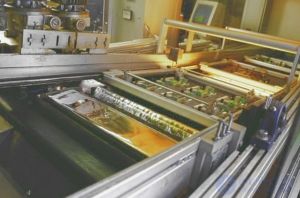
Wave soldering.
Wave soldering originated in the fifties in the UK. The technology is used for soldering output components located on one side of the board. Now it is the most common way to build large quantities of electronic modules. Wave soldering allows the use of domestic lead components, thanks to which this technology has become widespread in the CIS.
Wave soldering technology has a unique performance for automated installation of electronic components. At the same time, a series of operations are performed on the board: applying flux, preheating, washing off excess flux and drying. The board contacts the solder wave for a short time, which reduces the effects of high temperature. Due to the rapid heat transfer wave soldering is very effective when installing components installed in the metallized holes. Disadvantages of technology: a significant mass of solder permanently in the bath 100 ... 500 kg, significant size of the equipment about a few meters, a large oxidation of solder. The use of wave soldering technology places specific demands on the design of the board. Proper tracing of the conductive pattern reduces the likelihood of solder defects.
Boards have to be protected from solder waves. For this purpose, a layer of water-soluble film is applied to the board. To transfer the flux to the bottom surface of the board, it is foamed or sprayed. Molten solder soldering provides permanently present stationary wave. Boards with installed elements move across the waves. The best results are achieved by adjusting the tilt of the conveyor and the wave parameters. The angle of inclination of the conveyor is in the range of 5 ... 9 °. The speed of movement of the boards is selected based on the design of the assembled module, the soldering time of the components used, the pace of production, the preheating temperature. The movement of the assembled modules occurs at a speed of about one meter per minute. The remaining solder excess is blown away by a narrow stream of hot air. Purification of excess solder with air has received the name - air knife.
In order to form a ration of a skeletal form and high resolution, the solder should be applied on the soldering areas evenly with a thin layer. Different waves of different profiles are used: plane wave or wide, secondary or "reflected", delta wave, lambda wave, omega wave. Different number of waves allows to divide the equipment into categories: with one, two and three waves.
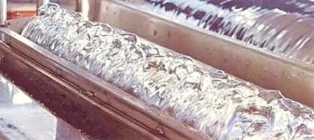
Two waves of solder.
With the technology of two waves, one wave is made narrow and turbulent. Vigorous movement of the solder in the first wave eliminates the formation of voids in the rations caused by the evaporation of the flux. The second wave cleans the board from the excess solder and completes the formation of a regular-shaped ration. Soldering temperature is in the range of 235 ... 260 ° C. Reducing the soldering temperature creates a more gentle thermal regime for parts of the assembled module. High temperatures are necessary when using lead-free solders and installing multilayer boards. To prevent oxidation of the joining surfaces, brazing is performed in a nitrogen atmosphere.
A wave of solder is created by mechanical and electromagnetic blowers, gas supply, and ultrasonic collisions. Mechanical supercharger works as follows. In the chamber with the nozzle with the help of the impeller constantly inject molten solder. The impeller is driven by an electric motor. Wave height is adjusted by changing the speed of rotation of the motor shaft. There is an easier way to create a solder wave. For this purpose, a gas is used that is fed under pressure into a closed cavity. But this method has its drawbacks. Intensive air movement through the solder leads to oxidation of the solder. The use of inert gas is unreasonably economical.
When the solder contacts the conductive board pattern and the component leads, a small amount of copper dissolves in the solder. A small amount of copper in the solder can disturb the eutectic of the alloy. The melting point of the solder increases, cold soldering occurs. To eliminate this phenomenon, copper and bismuth are included in the solder. Copper is previously added to the solder to saturation and a further increase in the copper content in the solder is impossible, and bismuth lowers the melting point of the solder.
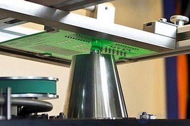
Селективная пайка с помощью сопла.
Селективная пайка появилась в девяностых годах. Селективная пайка - относительно новая технология, позволяющая производить избирательный монтаж только выводных компонентов. Метод требует минимум доработок для оптимизации печатных плат под данную технологию и позволяет монтировать большинство существующих типов выводных компонентов. Производительность монтажа в несколько раз выше, по сравнению с ручным монтажом.
Отличием селективной пайки от пайки волной является нагрев платы только в области пайки как при пайке паяльником. Удобно применять селективную пайку при сборке электронного модуля, содержащего планарные и малое количество выводных компонентов. Сейчас благодаря снижению использования выводных компонентов селективная пайка применяется все чаще. При сравнении с пайкой волной селективная пайка экономически более выгодна. По сравнению с пайкой волной селективная пайка не приводит к лишнему нагреву платы и позволяет применять больше типов компонентов, снизить вероятность появления дефектов, уменьшить подготовку к монтажу, исключается защитная маска, уменьшается износ оборудования отмывки плат. Внедрение селективной пайки позволяет сократить количество операций с платами, уменьшить время монтажа, уменьшить объем ручной работы. Возможна пайка разными припоями.
Селективная пайка проводится в несколько этапов. Вначале наносится флюс. Затем происходит подогрев флюса для подсушивания, активации и предотвращения термоудара при пайке. Последний этап – нанесения припоя. Весь процесс автоматизирован и происходит в специальной установке. Плата автоматически перемещается, проходя все этапы селективной пайки, начиная с нанесения флюса.
Технологии селективной пайки можно разделить на два основных типа в зависимости от применяемой головки с припоем. К одному типу технологии можно отнести использование сопла с припоем, над которым перемещается паяемая плата и происходит пайка всех точек поочередно. Ко второму типу можно отнести использование оснастки, образующей миниволны на нескольких соплах одновременно, расположенных в областях паек. Первый тип технологии более подходит для производства малых партий электронных модулей, второй для крупных партий. Пайка может осуществляться в среде азота.
Нанесение флюса выполняется тремя наиболее распространенными методами.
Флюсующий узел аналогичен головке струйного принтера и позволяет наносить флюс малыми порциями. В отличие от принтера узел нанесения флюса перемещается по плоскости как перо графопостроителя. Флюсуются только области пайки. Электромагнитный насос без механических деталей подает флюс в форсунку. Микрокапельная форсунка исключает попадание флюса на участки платы, расположенные вокруг области пайки. Точность нанесения флюса позволяет исключить операцию отмывки.
Флюсование распылением наносит флюс на всю плату. Количество форсунок наносящих флюс варьируется для каждого производимого электронного модуля.
Флюсование окунанием происходит с помощью ванны и адаптера с выдвижными насадками. Адаптер изготавливается для каждого производимого модуля индивидуально. Все области паек покрываются флюсом одновременно. Нанесение флюса окунанием актуально при изготовлении крупной партии. Адаптер с насадками меняется при переходе на другую плату. Применение насадок обеспечивает хорошее нанесения флюса точно на область пайки. Флюс хорошо наносится даже на труднодоступные точки пайки.
Нагрев платы выполняется различными нагревательными узлами.
Предварительный нагрев платы.
Инфракрасный нагрев выполняется с помощью нагревателей имеющих диапазон излучения от средних до коротких волн. Мощность каждого нагревателя измеряется в киловаттах. Нагрев может быть задан в соответствии с конструкцией печатного узла.
Нагревание кварцевыми излучателями и устройствами направленной конвекции. При использовании таких излучателей число задействованных источников тепла задается согласно ширине платы.
Пайка может выполняться одним соплом или множественной миниволной.
При технологии одного сопла плата перемещается с высокой точностью и позиционируется над соплом головки с припоем. Имеется возможность контролировать параметры каждого отдельного паяного соединения: высота насадки, волны, время нахождения в волне припоя и другие. На пайки в соответствии с программой расходуется строго заданное количество припоя.
Сопло для селективной пайки миниволной.
Различные сопла внутренним диаметром 1,5…20 мм позволяют сделать процесс пайки адаптируемым к производству большинства возможных электронных модулей. Если пайка производится в среде азота, то азот подается непосредственно в зону пайки.
Приспособление для селективной пайки множественной миниволной.
Пайка множественной миниволной обеспечивает повышенную производительность. Множественная миниволна пропаивает все необходимые точки пайки одновременно, и при этом качественно обрабатываются даже труднодоступные точки. При пайке множественной миниволной паяемые поверхности отлично смачиваются, образование перемычек минимально.
Selective soldering is unique in that the application of flux occurs in a pointwise and metered manner, the flux burns out during the soldering process and washing of the flux residues is not required. This saves on the process of washing the boards. This eliminates the need for cleaning equipment costs. Systems of selective soldering by laser and hot gas are being developed.

Comments
To leave a comment
Design and engineering of electronic equipment
Terms: Design and engineering of electronic equipment