Lecture
At a considerable distance from the television center or insufficient size of the received signal (even when using antennas with high gain), it is desirable to use an antenna amplifier to ensure reliable reception.
When purchasing an antenna amplifier, you should pay attention to the possibility of its installation near the antenna or on the antenna itself. Installed next to the TV, the antenna amplifier is not able to fully improve the reception quality of TV programs. It equally enhances both the TV signal and external noises: with a large noise level and a considerable length of the feeder line, high-quality TV viewing will not be possible.
The weak signal received by the antenna, passing through the feeder, will decrease even more and will be insufficient. Noises at the same time can reach considerable size. Therefore, you need to install the amplifier as close as possible to the antenna.
4. 2. 1. Unified television equipment (OTU-2. 2)
Equipment television unified OTU-2. 2 is used to work in collective television reception systems (TPCS). It provides amplification on television channels in the meter wavelength range and is designed for round-the-clock work on stairwells, at entrances (in antenna cabinets or directly on the wall).
The equipment includes:
- assembly housing with an addition filter KS-2;
- amplifiers UTD-I-II, UTD-III;
- power supply unit BPS-5 (BPS-3.2).
Depending on the version, one or two amplifiers are included in the equipment:
OTU-2.2.1: FTD-I-II ..................... 48.5 - 100 MHz;
OTU-2.2.2: FTD-III ....................... 174 - 230 MHz;
OTU-2.2.3: UTD-I-II and UTD-III .... 48.5-100 MHz and 174-230 MHz.
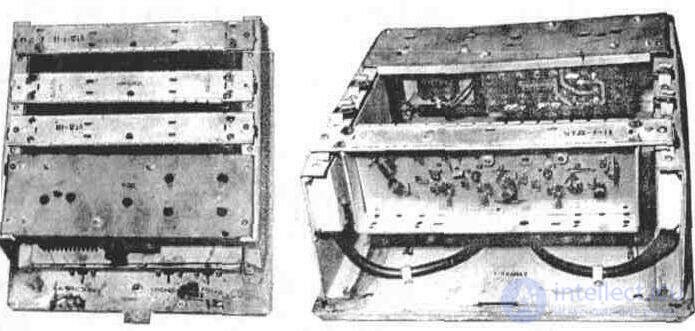
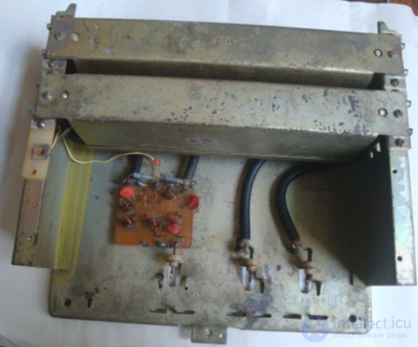
Fig. 4.9. OTU-2.2 appearance
Main technical characteristics of OTU-2. 2:
Gain, dB, not less ........................................... ............................ 25
Frequency response irregularity, dB, not more than, in the frequency bands:
each of the amplified channels .............................................. .............................. one
each of the amplified ranges .............................................. ........................ 3
KBV from the inputs and outputs of the equipment, not less .................................. 0, 5
Noise ratio, dB, not more than ........................................... .................................. 9
The output voltage (maximum) of each of the two signals applied to INPUT I (1-5 k) or INPUT II (6-12 k) of the equipment, with a cross-modulation factor of 46 dB, mV, no less ....... ............................................. 200
Power consumption from AC mains at a rated voltage of 220 V, W, not more than .................................. ..................... eight
Amplifiers UTD-I-II and UTD-III are designed to work as part of the OTU equipment. Structurally, they are made the same type and differ only in labeling.
A schematic diagram of an UTD-I-II amplifier designed to amplify television channels in the I-II range of meter waves is shown in Fig. 4. 10. The amplifier is made according to a three-stage scheme on transistors VT1-VT3 (КТ-368А). The first cascade is made according to the scheme with a common emitter, the second and third - according to the scheme with a common base. The modes of the transistors in the direct current determine the elements R2R3, R7R8, R12R13. Bandpass filters are used as matching circuits in amplifiers. The input circuit C1L1L2C2 provides the matching of the input impedance of the first amplifier stage with the characteristic impedance of the antenna. Correction of the frequency response block on the upper amplified frequencies is performed by the interstage filter L3C9L4C10.
Table 4. 1. These inductors UGD-I-II
Designation scheme | Number of turns | Wire brand and diameter, mm | Inductive., MH |
LI | 7, 5 | Sew-1, 0, 8 | 0, 33 |
L2 | 5, 5 | Sex -1, 0, 8 | 0, 2 |
L3 | 4, 5 | Sex -1, 0, 8 | 0, 33 |
L4 | 4, 5 | Sex -1, 0, 8 | 0, 31 |
L6 | 7, 5 | Sew - 1. 0, 8 | 0, 44 |
L7 | 7, 5 | Sex -1, 0, 8 | 0, 39 |
Coordination of the amplifier output with the input of the device of the addition of signals (CSS) performs the output bandpass filter L6C13L7C14. The supply voltage to the amplifier is supplied from the output high-frequency connector via L8C12L5C8C4.
Amplifier UTD-III is designed to amplify television channels in the III range of meter waves. The schematic diagram is shown in Fig. 4. 12. The amplifier circuit is made with CT-368A transistors. The first and third cascade are made according to the scheme with a common emitter, the second and fourth - according to the scheme with a common base. The modes of the transistors for the constant current determine the elements R1R2, R6R7, R9R10, R14R15. The input circuit C1L1L2L3C2 provides the matching of the input impedance of the first amplifier stage with the characteristic impedance of the antenna. Tuning for optimal matching is carried out by tanks C1, C2. Correction of the waveform response at the upper amplified frequencies provides interstage filter L4L5L7C11. Band-pass filter L10L8L9C18 matches the output of the amplifier with the input of the signal addition filter.
Table 4. 2. Data of inductors UTD-111
Designation scheme | Number of turns | Wire brand and diameter, mm | Inductive., MH |
L1 | 3.5 | Sew - I, 0.8 | 0.096 |
L2 | 2.5 | Sew-I, 0.8 | 0.055 |
L3 | 2.5 | Sew - I, 0.8 | 0.068 |
L4 | 3.5 | Sew-I, 0.8 | 0.048 |
L5 | 2.5 | Sex -1, 0.8 | 0.03 |
L7 | 1.5 | Sew - I, 0.8 | 0.078 |
L8 | 4.5 | Sew-I, 0.8 | 0.044 |
L9 | 1.5 | Sew - I, 0.8 | 0.045 |
L10 | 3.5 | Sew - I, 0.8 | 0.072 |
The inductors of the band-pass filters are made of wire sew -1-0, 8 without frames. The required value of inductance is achieved by changing the distance between the turns when adjusting the amplifiers.
The supply voltage to the amplifier is supplied from the output high-frequency connector through L 11С12C16C17L6C3C7C9.
The outputs of the amplifiers UTD-1-11 and UTD-111 are connected to the inputs of the signal combining device (Fig. 4.12). USS consists of upper filters C1L2C3L4C4 and low frequencies L1C2L3C5L5C6. The device of addition of signals provides isolation between amplifiers of different ranges (not less than 20 dB), introducing insignificant losses at operating frequencies (not more than 0.5 dB).
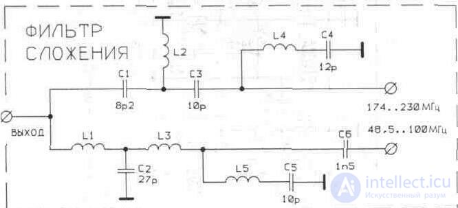
Fig. 4.12. Diagram of the device of addition of signals Table 4.3. Data inductance filter coils addition.
Designation scheme | Number of turns | Wire brand and diameter, mm | Inductive., MH |
L1 | five | Sew-I, 0.8 | 0.13 |
L2 | 2.5 | Sex -1, 0.8 | 0.05 |
L3 | five | Sew-I, 0.8 | 0.118 |
L4 | 6 | Sew-I, 0.8 | 0.16 |
L5 | four | Sew-I, 0.8 | 0.102 |
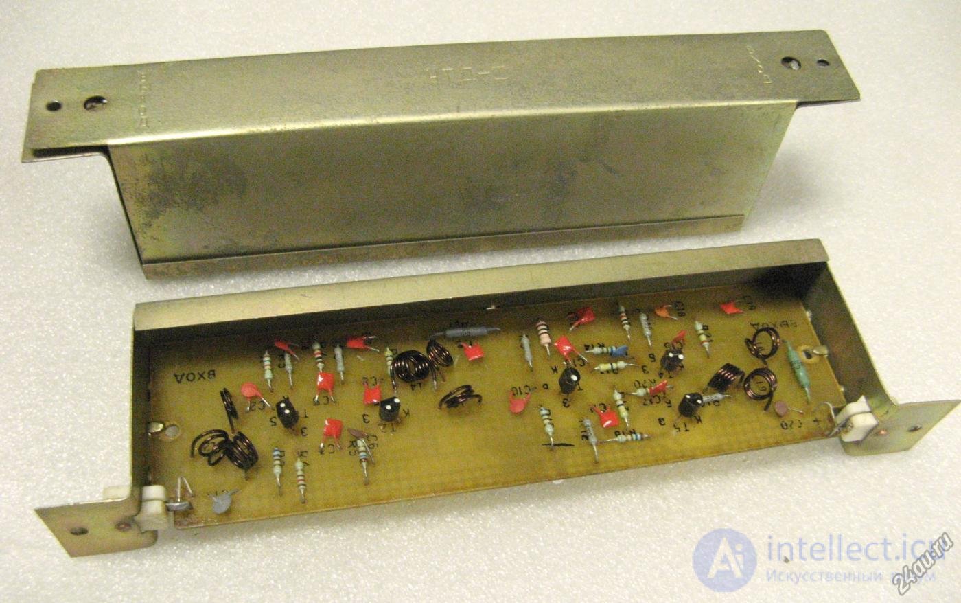
The power supply unit BPS-5 is designed as a removable functionally complete unit. A metal transformer, a rectifier and a stabilizer board, a regulating transistor with a cooling radiator and a fuse holder are fixed on a metal base.
Table 4.4. The winding data of the power transformer BPS-5
Wire brand | PE-1 | Sew-1 |
Copper diameter | 0.12 | 0.44 |
The number of turns | 4100 | 380 |
Retraction | 2370 | - |
Winding type | turn to turn | turn to turn |
Winding direction | one way | one way |
Insulation between layers | CT-50.1 layer | CT-50, 1 layer |
Insulation top winding | K-120, in 2 layers | K-120, in 2 layers |
Winding procedure | primary | secondary |
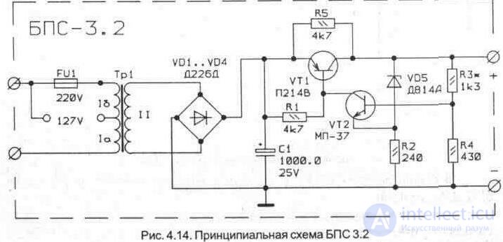
The schematic diagram of BPS-5, shown in Fig. 4.13, made according to the traditional parametric stabilizer scheme with a regulating transistor.
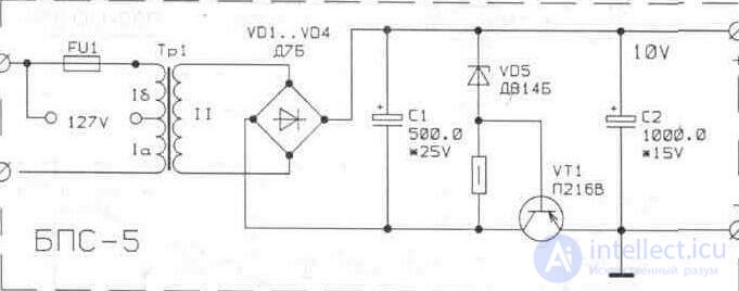
Fig. 4.13. Schematic diagram of BPS-5
In later releases of the equipment, the power supply unit BPS 3.2 is used (Fig. 4.14).
Main technical specifications
Output Voltage, V .............................................. ............................................. 10 ± 0,4
Maximum permissible load current, A, not less than ......................................... ......... 0.3
Output voltage ripple, mV ............................................. ...................... 2
The power consumed from the network, W, not more than ........................................ ................ eleven
The power supply circuit provides protection against short circuits and overloads, which is triggered if the load current exceeds the maximum permissible value by 100%. In the normal stabilizer mode, an increase in the load current leads to an increase in the emitter current of the transistor VT2 and to a decrease in the current through the D814A Zener diode. Total emitter current VT2 plus current Zener diode with increasing current
load decreases. In this mode, with voltage fluctuations at the load, the base-emitter circuit of the transistor VT2 receives a voltage with a polarity corresponding to negative feedback. When an overload occurs, the current through the zener diode stops, which is equivalent to the rupture of the shoulder of the bridge formed by the zener diode. As a result, the polarity of the voltage at the base of the transistor VT2 is changed to reverse, the feedback becomes positive and the transistors are closed. To convert the circuit to stabilization mode, you must turn off the BPS 3.2 and then turn it on after eliminating the causes of the overload.
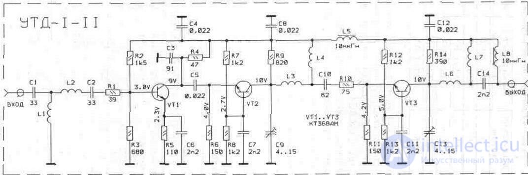
Fig. 4.10. Schematic diagram of the amplifier UTD-I-II
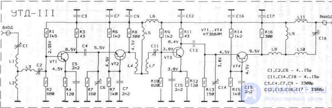
Fig. 4.11. Schematic diagram of UTD-III
Table 4.5. The winding data of the power transformer BPS 3.2
Number of windings according to the scheme | Core | The number of turns | The wire |
la | SHL 16x16, ribbon | 1700 | PEV-1, 0 0.23 |
1b | SHL 16x16, ribbon | 1300 | PEV-1, 00.2 |
II | SHL 16x16, ribbon | 270 | PEV-1, 0 0.55 |
4.2.2. Unified television equipment (OTU-3. 2)
Unified television equipment OTU-3. 2 is used for work in the system of collective reception of television SKPT and provides the ability to receive programs of meter and decimeter ranges (using the converter KTK). The equipment is designed for round-the-clock work on staircases, entrances (in antenna
closets or directly on the wall).
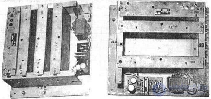
Fig. 4.15. Appearance of OTU-3.2
antenna amplifier UTD-I-II, UTD-III
Main technical specifications
Gain for each input when picking:
converters КТК, dB, not less ........................................... ..................... 24
UTK amplifiers 1-5 channels, dB, at least ....................................... ........ 34
UTK 6-12 channel amplifiers, dB, at least ....................................... ...... 29
UTD amplifiers, dB, not less ........................................... ....................... 25
Uneven frequency response in the frequency band of each of
amplified channels, dB, not more than ........................................... ............................ 2
Equipment CWS from the input side, no more .......................................... ......... 2
Noise figure, dB
in the I-II range of 48.5-100 MHz, no more than .................................... ............. eight
in the III band 174 - 230 MHz, no more ........................................ ........... 9
Maximum output level of TV channel gain, dB / µV, no less than ........ 106
AC power consumption
with a rated voltage of 220 V, W, no more than ........................................ ........... 12
Maximum number of converters and amplifiers installed
when completing the equipment:
KS-3 body, no more ........................................... ................................... 3
KS-4 body, no more ........................................... ................................... four
Amplifiers UTD-I-II, UTD-III UTK-1 (2 .... 12) are of the same type and are externally marked by marking. The schematic diagrams of the UTD-I-II and UTD-III amplifiers are similar to those used in the OTU 2. 2 and are described in
section 4. 2. 1. The description and schematic diagram of the CPC converter are given in sec. 4. 4. 1.
A diagram of a typical UTK-1 channel amplifier (2 .. 12) is shown in fig. 4. 16. According to this scheme, amplifiers are performed on any of the twelve TV channels. UTK have different values of the elements (table. 4. 6), depending on the channel gain.
Table 4. 6. The number of turns of the coils and the capacitance of the capacitors of the transistor antenna amplifiers UTC
Designation scheme | Unit | The number of turns of the coils and the capacity of the capacitors for | TV - | kana la | |||||||||
measuring | one | 2 | 3 | four | five | 6 | 7 | eight | 9 | ten | eleven | 12 | |
L1 | turns | 7 | 7 | 7 | 7 | 6, 5 | five | 4, 5 | 4, 5 | four | four | four | four |
L2 | turns | 7 | 7 | 7 | 7 | 6, 5 | five | 4, 5 | four | four | 3, 5 | 3, 5 | 3, 5 |
L3 | turns | 6, 5 | 6, 5 | 6 | 6 | 5, 5 | 3, 5 | 3, 5 | 3 | 3 | 2. 5 | 2, 5 | 2, 5 |
L4 | turns | eight | eight | 7 | 7 | 7 | 5, 5 | 4. 5 | 4, 5 | •four | four | four | four |
L5 | turns | 6, 5 | 6, 5 | 6 | 6 | 5, 5 | 3, 5 | 3, 5 | 3 | 3 | 2, 5 | 2, 5 | 2, 5 |
L6 | turns | eight | eight | 7 | 7 | 7 | 5, 5 | 4, 5 | 4, 5 | four | four | four | four |
C1 | pf | 15 | ten | 6, 8 | 4, 7 | 4, 3 | 2 | 2 | sixteen | 18 | sixteen | sixteen | 15 |
C2 | pf | 22 | 15 | 6, 8 | 5, 6 | 5, 6 | 2, 2 | 2. 2 | 2 | 2 | 2, 4 | sixteen | sixteen |
C7 | pf | 15 | 9, 1 | 5, 1 | 4, 7 | 3, 6 | 18 | sixteen | 14 | 12 | 2, 2 | 13 | one |
C8 | pf | 18 | 6, 2 | 5. 1 | 4, 7 | 3, 6 | 13 | sixteen | 15 | 18 | sixteen | 13 | 13 |
C13 | pf | 18 | 9, 1 | 6, 2 | 4. 7 | 3, 6 | 18 | sixteen | 14 | 12 | 2, 2 | 13 | one |
C14 | pf | 12 | 7, 5 | 6, 8 | 4, 7 | 3, 6 | 15 | 2 | 2 | 18 | sixteen | sixteen | sixteen |
C17, C18, C19 | pf | 2, 4 | 2, 4 | - | - | - | - | - | - | ||||
Note: All inductors are wound with PEV 0, 47 wire on organic glass frames with a pitch of cut spiral grooves of 0, 5 mm. For 1–5 channels, the frame diameter is 10 mm, for 6–12 channels, 8 mm.
The channel amplifier is made on a four-stage scheme on GT 313B transistors (in later versions of amplifiers, other transistors are used). The first and third cascades are made according to the scheme with a common emitter, the second and fourth - according to the scheme with a common base. Modes of transistors for DC determine the elements of R1, R2, R3, R4, R8, R9, R12, R13, R17, R18. The change in the current of the transistor VT1 using a potentiometer R4 adjusts the magnitude of the output signal of the amplifier. The gain bandwidth of the specified channel is adjusted using the contours of the bandpass filters C1L1L2C3, C9L3L4SP, C16L5L6C18. Capacities C2, C10, C17 are used to provide the necessary connection between the circuits in amplifiers UTK-1 and UTK-2. Circuits C1L1, L2C3, L4C11, L6C18 are made according to a serial circuit, and C9L3, C16L5 - according to a parallel circuit. The inclusion of the band-pass filter circuits in parallel and in series allows the high output impedance of the transistor of the previous stage to be matched with the low input impedance of the transistor of the next stage, or the characteristic impedance of the cable at the amplifier's output. The supply voltage to the amplifier is supplied from the output high-frequency connector via L7C15, R11C8.
Electrical parameters of amplifiers channel UTK
Amplifier parameters for TV channels ............................................. ................. 1 ... 5 .. 6 ... 12
Gain at the channel average frequency, dB, at least ..................... 34 ...... 29
Irregularity of the frequency response in the channel frequency band,
dB, not more than .............................................. .................................................. ........... 1, 5 ...... 1, 5
SWR in the channel frequency band, no more than .......................................... ....................... 1, 7 ...... 1, 7
Noise ratio, dB, not more than ........................................... ............................... 5 ......... 9
18 MHz off-band selectivity
amplified signal, dB, not less than ........................................... ........................ 20 ...... 20
Maximum output level in the TV channel, dB / µV, not less ................. 110 .... 103
Power consumption, W, not more than ........................................... ....................... eleven
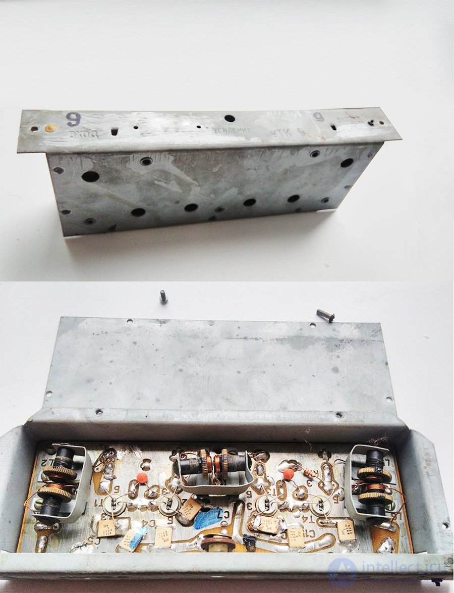
Fig. 4. 17. The appearance of the amplifier range UTK
All considered devices are designed to work together in a single assembly package in combinations determined by specific conditions. The devices are powered from a common source, which is part of the equipment. Since the supply voltage is supplied to the amplifiers and converters through the high-frequency output connector, elements are included in the assembly case to ensure the separation of direct current and high-frequency current.
The power supply unit in OTU 3. 2, equipped with a KS-4 case, is made according to a simplified scheme on a single transistor. Structurally, the network transformer and stabilizer board are installed on the KS-4 case.
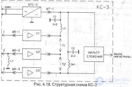
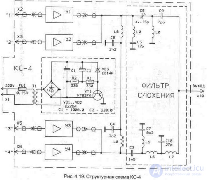
The schematic electrical diagram of the OTU 3. 2 connections, when equipped with the KS-3 housing, is shown in fig. 4. 18, when equipped with a KS-4 case in fig. 4. 19.
The differences between the channel amplifiers of the last years of production (Fig. 4. 20, 4. 21) consist in the use of higher-frequency transistors and minor changes in the circuit.
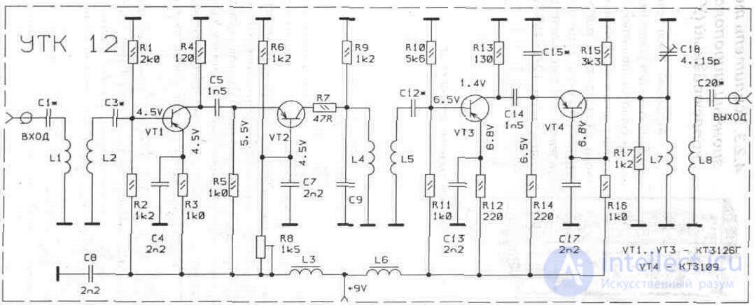
Fig. 4. 21. Schematic diagram of UTK-12
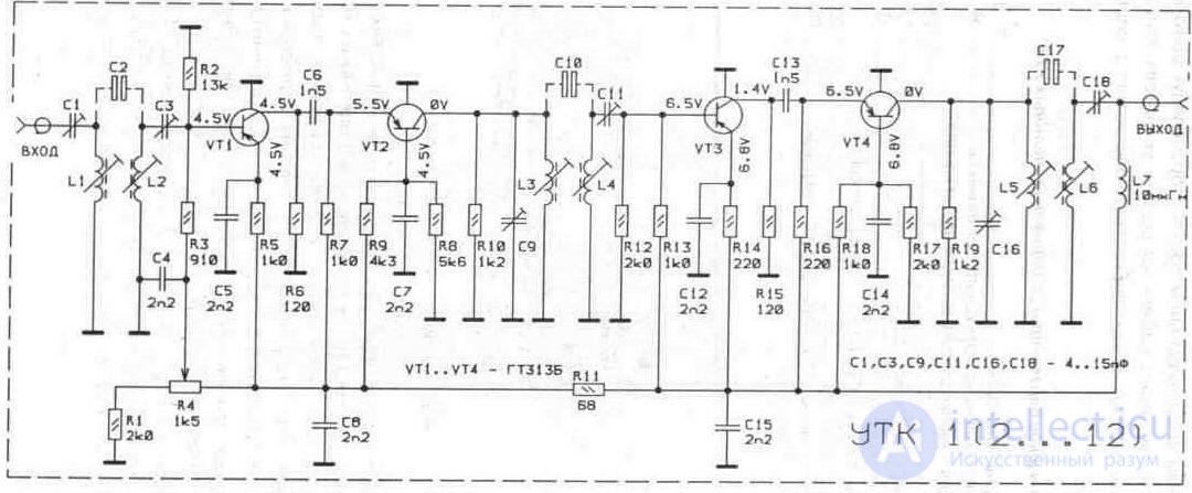
Fig. 4.16. Schematic diagram of UTK-1 (2 ... 12)
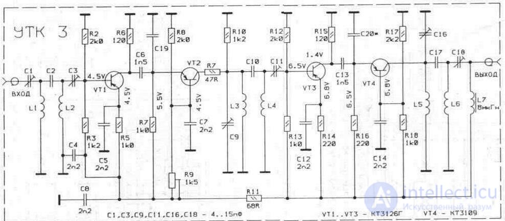
Fig. 4.20. Schematic diagram of UTK-3

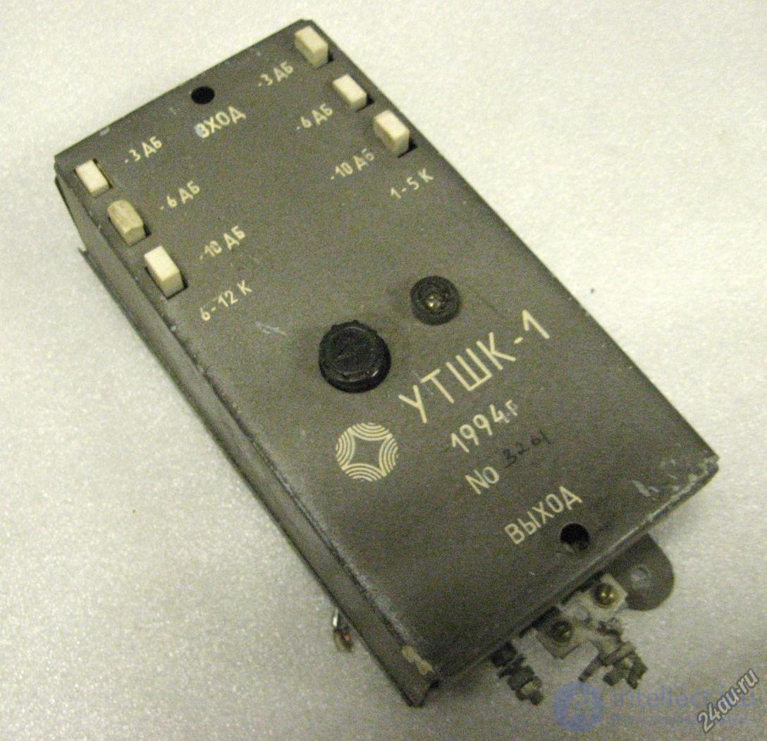
4. 2. 3. Amplifier television broadband collective (UTSShK)
Antenna amplifier (UTSShK) is designed to amplify television signals received by common use antennas of the metro range, and is designed for round-the-clock operation from an AC network with a frequency of 50 Hz, voltage 127 ± 15% or 220V ± 20%.
Fig. 4. 22. The appearance of the amplifier UTSHK
Main technical characteristics of UTShK
Amplifier parameters for ranges .............................................. ...................... I-II ....... Ill
Gain, dB, not less ........................................... .......................... 25 ....... 25
Irregularity of the frequency response, dB, no more ........................................... ............................. 2 ......... 3
SWR from the entrance side, no more ........................................... .................................. 1, 8 ....... 2
Noise ratio, dB, not more than ........................................... ................................. 8 ......... 9
Maximum output level in the TV channel, dB / µV, not less than ..................... 110 ..... 106
Power consumption from AC mains at a rated voltage of 220 V, W, not more than .................................. ............................. eight
Structurally, the amplifier is made in a metal case divided by two partitions. In the central compartment, there is a power transformer, a stabilizer board (UZ) and a signal combining device (U4), in the side compartments there is an amplifier line of UTD-I-II (U1) and UTD-III (U2). The antenna inputs and the common output are located on opposite sides of the housing. The diagram of the amplifier line U1 is shown in Fig. 4. 23. The description of the concept is similar to the amplifier UTD-111, used in the OTU, with the exception of some elements and their designations.
Diagram of the line U2 is shown in Fig. 4. 24. A distinctive feature of the circuit diagram of the U2 line from the UTD-III amplifier used in the OTU is the execution of the terminal stage on two transistors VT4, VT5 with parallel switching on the output, which increases the load capacity of the amplifier.
The US stabilizer (Fig. 4. 25) is made on transistors VT1, VT2. The output transistor of the stabilizer VT1 (for heat dissipation) is installed on the amplifier body.
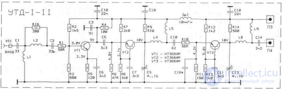
Fig. 4. 23. Schematic diagram of the line U1 (UTSShK)
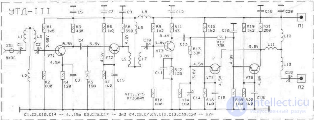
Fig. 4. 24. Schematic diagram of the line U2 (UTSShK)
Fig. 4. 25. Schematic diagram of the power supply UTShK
The outputs of the amplifier bars are connected to the input of the V4 board - a signal combiner (USS). The device for adding signals (Fig. 4. 26) is a high-pass filter (L2, C2, C4, L4, C6) and low frequencies (C1, L1, C3, L3, C5, L5).USS provides isolation between the ranges of amplifiers of different ranges (not less than 20 dB), introducing insignificant losses at operating frequencies (not more than 0, 5 dB). Adjustment of the frequency response in the III range is made by adjusting the capacitances C4 (U4) and C19 (U2).

Fig. 4. 26. Schematic diagram of the filter unit UTShK

Comments
To leave a comment
Television and antennas. Theory. Broadcast and cable. Digital and analog
Terms: Television and antennas. Theory. Broadcast and cable. Digital and analog