Lecture
An electronic device designed to increase the parameters (current, voltage, power) of an electrical signal is called an amplifier.
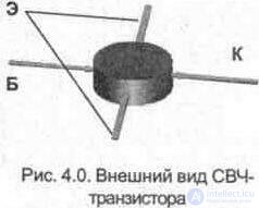
The main amplifying element in the circuits of antenna amplifiers is a high-frequency transistor, which is selected according to the characteristics when designing specific circuits for the MB and UHF TV broadcast bands.
The operating mode of the selected transistor in a particular projected circuit differs from the parameters given in the specifications. The value of most parameters depends on the operating mode and temperature, and with an increase in temperature, their dependence on the mode is more pronounced. In reference books, as a rule, typical (averaged) dependences of transistor parameters on current, voltage, frequency, etc. are given.
Very important parameters when choosing transistors for antenna amplifiers are: cut - off frequency - frp, noise factor - Ksh, voltage gain factor - Ki and some others.
The deterioration of the characteristics of transistors at frequencies close to frp. due to technological capabilities and their electrical strength (permissible base thickness, gate length). With increasing frequency, the influence of the parasitic parameters of transistors increases:
interelectrode capacitances, inductances of the terminals, base resistance, etc. Increasing the input resistive conductivity of the transistor reduces the gain of the antenna amplifier and increases Ks, therefore it is necessary to reduce the inductance of the emitter output and connecting wires. To do this, in the microwave transistors make two flat short output of the emitter, which is usually soldered directly to the bus of zero potential ("earth").
In amplifiers, by changing the mode of the transistors and coupling to the source and load, you can achieve maximum gain or minimum noise figure. The noise level of transistor antenna amplifiers depends on how they are
construction and mode of operation, the magnitude of the resistance of the source of signals. Reducing the noise of bipolar transistors is achieved by reducing the collector current I to and base current Ib (without a significant reduction in current transfer coefficient h21, as well as the use of transistors
with a high limiting frequency fv and low resistance rb . The transistors are chosen so that the condition is met
fв <= 0,1fгp, (4.1)
where: fgp is the cutoff frequency of the current transfer ratio in the circuit with a common emitter.
The use of transistors with a low noise figure, the fulfillment of the condition of matching them with the source and load, and the selection of the optimal operation mode are the main ways to increase the sensitivity of antenna amplifiers.
Three circuits of switching on the amplifying element (transistor) are most common.
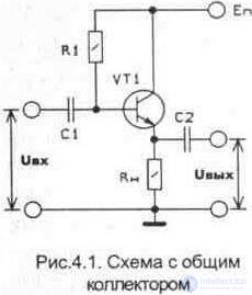
In circuits with a GENERAL COLLECTOR (OK) and a GENERAL DRAIN (OS), the voltage transfer ratio is close to unity, and the output signal in magnitude and phase repeats the input signal (Uex x = Uxx). These cascades are called “voltage repeaters” (emitter or stock repeater). Such a circuit provides a low input capacitance and the largest input resistance, which greatly increases with increasing load resistance. The output impedance of the circuit is the smallest. These schemes are used as matching and separation, providing signal transmission from high-resistance sources to low-resistance circuits and cascades.
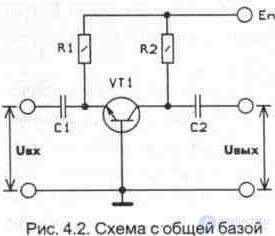
In circuits with a TOTAL BASE (OB) and TOTAL SHUTTER (03), the output current is approximately equal to the input current, so they are called “current repeaters”. Such a circuit has a large input conductance (low input resistance), the largest output resistance compared to other schemes and provides mainly voltage gain. The current gain does not change much with changes in operating mode, temperature, and replacement of transistor instances. The low input capacitance of the circuit improves the cascade parameters (ON, 03) at high frequencies, although a small input impedance is a disadvantage of these circuits.
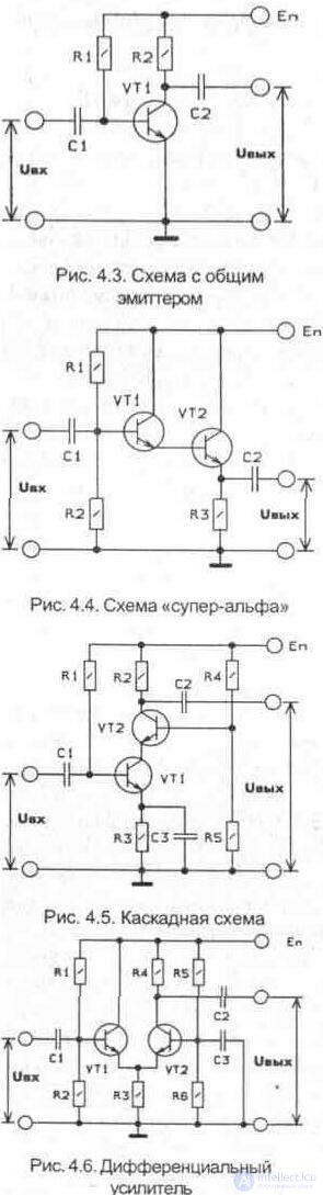
The scheme with GENERAL EMITTER (OE) for bipolar and, GENERAL SOURCE (OI) for field-effect transistors provides the greatest gain in power, but changes the phase of the output voltage by 180 ° with respect to the input. As the load resistance increases, the input resistance decreases. These circuits are used in cases when with the minimum number of transistors is required to obtain the greatest gain. However, the input capacitance of the SEB transistors affects the narrowing of the bandwidth at high frequencies.
One of the effective methods to increase the input resistance of the emitter follower is to increase the current transfer coefficient of the transistor h21e. In the "superalph" circuit (also called the Darlington circuit), the emitter current of the first transistor controls the base of the second transistor, and therefore the resulting current transfer coefficient h21e is equal to the product of current transfer coefficients of individual transistors. From here
Zin = h21e * h21e * Re. (4.2)
By various combinations of cascades, it is possible to construct other amplifying circuits:
OE = OB - cascade scheme with sufficiently small internal noise, and high stability;
OK = ON - differential amplifier, which has the advantage over compensation of voltage U be of both transistors in comparison with the cascade circuit.
4. 1. 1. Schematic features of antenna amplifiers
When amplifying weak television signals, the intrinsic noise level of the amplifier's input stages is of great importance. Therefore, in microwave antenna amplifiers using microwave transistors with low values of noise parameters. The noise parameters of antenna amplifiers are also influenced by the parasitic parameters of the passive elements used - resistances and capacitances.
Broadband antenna amplifiers are designed to amplify signals in the frequency band of several meter and (or) decimeter wave bands. Typically, a broadband amplifier is built on the basis of a resistive amplifier stage, which has the most uniform frequency response in a relatively wide frequency range. To extend the bandwidth in the direction of low and high frequencies, special correction circuits are introduced into the circuit. However, the characteristics of transistors are degraded at high frequencies, which leads to a narrowing of the bandwidth of the amplifiers at these frequencies. In narrowband amplifiers (within the bandwidth), the change in the characteristics of the transistors can be neglected.
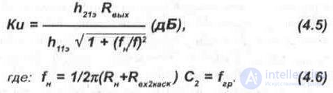
Aperiodic (resistive) amplifier with a capacitive coupling is also called an RC amplifier. The name of the circuit is associated with the nature of the load resistance RH and the capacitive coupling of the cascade with the signal source, or with the previous cascade (or the load of the next cascade). Aperiodic amplifiers provide high gain stability and high sensitivity when amplifying weak signals. The gain in the high frequency range can be calculated by the formula:
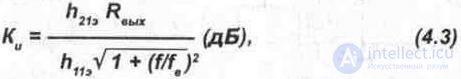
where f is the frequency for which the gain is determined;
Rout - resistance obtained by parallel connection Rn + Rвx2;
fv = fgp:
fv = 1/2 l * Req * Co, (4.4)
where Req = the sum of the resistances that shunt the output stage. Co is the sum of the capacities that shunt the output stage.
The gain in the low frequency range can be calculated by the formula:
Election amplifiers are called amplifiers whose bandwidth (retention) is narrowed to separate signals in the desired frequency band from signals, interference, or noise from other frequencies. According to the principle of operation and circuit design, selective amplifiers can be divided into resonant, bandpass, etc. Resonant amplifiers are designed to amplify signals in a given narrow frequency band. Their main feature is that the cascade load is frequency-dependent, which is a parallel LC circuit tuned to the frequency of the amplified signal. The oscillatory circuit can be included in the amplifier according to the transformer, autotransformer, capacitive circuit.
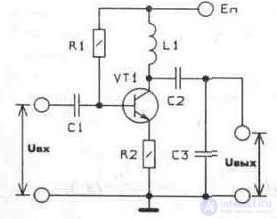
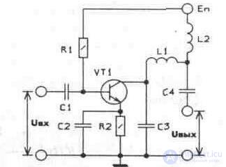
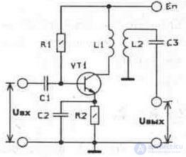
Fig. 4. 7. Methods of matching in selective amplifiers
The larger the Q-factor of the circuit, the narrower the bandwidth of the amplifier, the greater the gain. By connecting a resistance parallel to the resonant circuit, it is possible to reduce its Q-factor and thereby affect the gain and the bandwidth of the amplifier. An additional advantage of selective amplifiers compared to aperiodic is the compensation by tuning the oscillatory circuits of the influence of parasitic capacitances of the installation, which reduce the gain at high frequencies. By increasing the impedance of the load, they compensate for parasitic capacitive influence, thereby increasing the gain. The latter is carried out with a selection distributed in amplifier stages or concentrated in one stage using a concentrated selection filter (FSS).
4.1.2. Requirements for amplifying devices
The parameters that characterize the circuits of amplifiers include the gain, the unevenness of the gain, the band of amplified frequencies, etc.
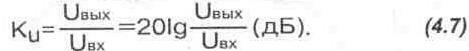
GAIN RATIO (K) of the amplifier is the ratio of the output value to the input. Depending on the considered electrical value, there are voltage gain factors. current and power.
VOLTAGE AMPLIFIER (Ku) is the ratio of the voltage at the output of the amplifier to the input:
The voltage gain in multi-stage amplifiers is equal to the product of the gains of each stage:
Total = K1 K2 K3 ... (in relative units) or
Kobsch = K1 + K2 + K3 + ... (dB).
CURRENT AMPLIFIER COEFFICIENT (Ki) - this is the ratio of the output current to the input:
. Ki = Iout / Iin = 20lg (Iout / Iin) (dB). (4.8)
COEFFICIENT AMPLIFICATION ON POWER (Cr) is the ratio of output power to input:
Cu = Pout / Pin = 10lg (Pout / Pin) (4.9)
UNEQUALITY OF THE GAIN COEFFICIENT - the value characterizing the change in the gain factor within the operating frequency range. It is defined as the ratio of the maximum gain to the minimum in the band of amplified frequencies.
Amplitude frequency response (AFC) - the dependence of the gain or amplitude (voltage) at the output of the amplifier on the frequency of the input signal, constant in magnitude. Since the parameters of the elements of the amplifiers depend on the frequency, the magnitude of the output signal will be constant only in a certain frequency range, called bandwidth.
TRANSMISSION STRIP (V) or RANGE OF AMPLIFIED FREQUENCIES - frequency range in which the gain factor changes no more than is allowed by the technical conditions. Allowable gain changes within the passband depend on the purpose and conditions of the amplifier. It is usually considered permissible to attenuate the signal level by 3 dB (2 ^ 0.5 = 0.707 times) compared with the maximum value at the resonant frequency (s). The bandwidth is defined as the difference between the upper fc and the lower fn boundary frequencies. B = fv-fn. (4.10)
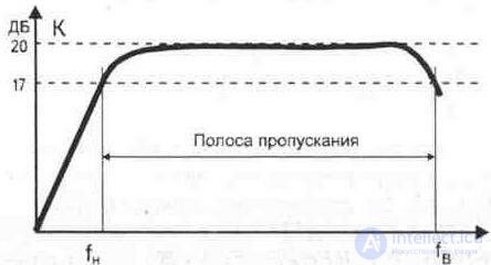
Fig. 4.8. Amplifier bandwidth
Depending on the purpose, antenna amplifiers can be relatively narrow-band [bandwidth less than an octave, fv / fn <2] and broadband [a band is several octaves].
DYNAMIC RANGE (D) - the range of levels of amplified input signals, limited by self-noise from below and from above by permissible non-linear signal distortions:
D = 20 lg (Uin.max / Uin.min) (dB). (4.11)
NOISE RATIO [F] is a parameter of the receive (transmit) channel, expressed as the ratio of signal power to noise power and allows numerical evaluation of the noise characteristics of devices (in most cases, the parameter value is specified in decibels).

Comments
To leave a comment
Television and antennas. Theory. Broadcast and cable. Digital and analog
Terms: Television and antennas. Theory. Broadcast and cable. Digital and analog