Lecture
The prerequisites of creation are the presence of the production of bipolar and unipolar transistors, the theory of calculating such transistors Shockley, Desey and Ross, Tesner. Developments of the head transistor institute - NII-35 (NII "Pulsar"). In the domestic technology of development and production of transistors, the period up to the beginning of the 60s is characterized by the use of single-crystal germanium as a source material and the release of only bipolar transistors. Unipolar transistors were not released. The technology of integrated circuits required the presence of both types of transistors as active elements of microelectronic circuits of various functional purposes and the introduction of silicon single crystal technology. In the period 1957–1961 The author developed germanium unipolar transistors of the 339 series, and on the basis of these works the dissertation was defended.
The concepts of miniaturization and microelectronics development are micromodular equipment and the US Tinkertoy project of the US Army, mastered in KB-1. Simultaneously with the development of the production of bipolar transistors and their use in defense and space technology, the Lead Transistor Scientific Research Institute-35 developed the technology and technology of their circuitry application, primarily as the standard design circuit elements of the micromodule program - the main developers of Barkans (KB-1) and Nevezhin (SRI-35). It was based on the principles of miniaturization of transistors and radio components, as well as the principles of assembly automation from miniature standard parts of a set of standard blocks of various circuits (like the Tinkertoy project of the US Army).
Mastering critical technology on silicon - a planar silicon technology. IEP. A strategic breakthrough in the United States in the field of transistors and integrated circuits should be considered the development and production implementation of technology on silicon, especially such critical technology as planar. In domestic production practice, the development of planar technology was practically started only in 1962 from the zero level.
A significant impetus to the development of the work was the invention of silicon integrated circuits in 1959 in the US by Jack Kilby and their production by the American company Texas for use in the Minuteman rocket guidance system. Attempts to create three-dimensional integral domestic schemes in Germany were made by the author at NII-35 in 1959–1962. Since 1959, the development of domestic silicon integrated circuits, in fact, represented a continuous process of competitive correspondence with Jack Kilby.
Concepts of repetition and copying of American technological experience - the methods of the so-called "reverse engineering" of the IEP operated. Prototype samples and production samples of silicon integrated circuits for reproduction were obtained from the USA, and their copying was strictly regulated by the orders of the Ministry of Environmental Policy (Minister Shokin). The concept of copying was tightly controlled by the minister for more than 19 years, during which the author worked in the IEP system, until 1974.
This applied not only to the development of microelectronics, but also to the creation on its basis of computer equipment, for example, during the reproduction of computers of the IBM-360 series - (the domestic series "SERIES 1-2"). The most technological assistance was provided by the process of copying real US-made silicon silicon integrated circuits. Copying was carried out after depressurization and removing the cover from the sample, copying a flat (planar) pattern of transistors and resistors in the circuit, and also after examining under the microscope the structure of all functional areas. The results of copying were issued in the form of working drawings and technological documentation.
The creation of the first Russian silicon integrated circuit was focused on the development and production with military acceptance of a series of TS-100 integrated silicon circuits (37 elements - the equivalent of the circuit complexity of a trigger, an analogue of the American IC of the SN-51 series by Texas Instruments). The work was carried out by SRI-35 (director of Trutko) and the Fryazinsky plant (director of Kolmogorov) by defense order for use in an autonomous altimeter of a ballistic missile guidance system.
The development included six typical integrated silicon planar circuits of the TS-100 series and with the organization of pilot production took three years at SRI-35 (from 1962 to 1965). It took another two years to master the factory production with military acceptance in Fryazino (1967). An analysis of the implementation of the planar technology cycle (over 300 technological operations) in domestic practice showed that this critical technology had to be mastered from the zero level and practically independently, without outside help, including on technological equipment. A team of 250 people in the scientific and technological department of the Scientific Research Institute-35 and an experimental workshop specially created at the department worked on solving this problem. At the same time, the department served as a training ground for specialists from many IEP enterprises that mastered this technology. For example, specialists of the semiconductor plant of the 2 nd Main Directorate of the IEP in Voronezh (Kolesnikov’s director, Nikishin, the moderator) studied in this department.
The main attention in the development of planar technology was paid to the production development of industrial photolithography techniques with high optical resolution, up to 1000–2000 lines per millimeter. These works were carried out in close cooperation with optical specialists from LITMO (Kapustin) and GOI (Leningrad).
The development of the planar technology automation department and the design of special process equipment (lead designer Zakharov) also played a major role. Developed automated units for the operational processing of silicon technological plates (washing, applying photoresist, conveyor oxidation, etc.) based on the use of pneumatic automation and pneumonics.
In 1964, the scientific and technological department of NII-35 for the development of integrated circuits was visited by the Chairman of the MIC Smirnov. After this visit, the department received Japanese scientific equipment, which was used in promising developments. In the spring of 1965, a visit was made to the experimental workshop of the scientific and technological department of NII-35 for the development of silicon integrated circuits by the Chairman of the Council of Ministers of Kosygin. During the period of development from 1962 to 1967, the author, as head of the department, had to repeatedly report on the progress of work to the Chairman of the State Committee for Science and Technology and Deputy Director of the Department. Chairman of the Council of Ministers Rudnev, President of the Academy of Sciences Keldysh, and also to be in constant contact with the department of science of the military-industrial complex and the defense department of the Central Committee, while the department of aviation equipment of the Ministry of Defense, who led the organization of military acceptance.
Creating Zelenograd . Zelenograd is a center of microelectronics consisting of 6 enterprises with pilot plants, the domestic equivalent of Silicon Valley in California. The author at the beginning of 1963 gave a course of lectures to the current director of Zelenograd, deputy. The Minister of IEP F.V. Lukin, on the basis of which technical proposals were prepared for the development of semiconductor mechanical engineering for Zelenograd, in particular, for thermal processes and photolithography (for the director Savin), for the procurement of technological equipment for imports (the Nazaryan and Struzhinsky groups), including including for an experimental plant in Fryazino.
The results of the author's development are recorded and confirmed by a number of scientific and technological reports of the Scientific Research Institute-35, copyright certificates, a number of articles published in the collections “Semiconductor devices and their use”, “Microelectronics” and published books and brochures for the period before 1974.
TsM immediately began to create a fundamentally new product. Already in May 1963, the first samples of vacuum spraying equipment were developed at the NIITM. In the second half of 1963, the first results on thin-film technology were already obtained at the NIIMP. It was necessary to test them on a real product and publicly demonstrate the capabilities of microelectronics. We decided to use the idea already tested by Staros - to make a micro receiver. Recalls I.N. Bukreev: “The first model, Micro, was a direct gain receiver, while the second was a bit larger, already superheterodyne. He had a very sharp tuning, and since in the USSR there were very few radio stations on medium and long waves, this seemed like a drawback. But when in 1964 I brought this receiver to the United States at the congress of radio engineers, it made a world sensation there! Newspaper articles, photographs: how the USSR was able to overtake us? ... in New York, where there were about 30 local radio stations, the sharp tuning of our receiver was just right. “Micro” were then sold for currency also in France, England, and everywhere there it stood in line in the 60s. In general, Micro was the first sensation for leadership. Khrushchev took them abroad as souvenirs, presented to G. Nasser, Queen Elizabeth ... ”[9].
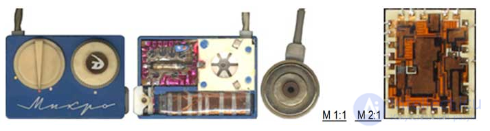
Fig. 3 M 1: 1 M 2: 1 The first microelectronic product in the USSR - the Micro radio (full-size photo of the receiver). The size of the receiver 43v30 is 7.5 mm (without protruding controls). Listen to the radio broadcast through the phone for the hearing aid inserted into the ear (third from the left).
Fig. 4. The first series of IP in the USSR, “Path”,
thick film, upper row, “Ambassador”,
thin film, bottom row.
(Left and center - in double size,
on the right - full size).
The “Micro” radio receiver (Fig. 3), made using thin-film technology, became the country's first serial microelectronics product. It was developed in the second half of 1963 at the NIIMP. And in 1964, its production was mastered by releasing about 80 thousand units, after which it was transferred to the plant of the large-scale industrial complex in Minsk. Until the mid-seventies, this micro receiver could be bought in stores in the USSR and France.
In 1964, NIIP began to create a series of thick-film GIS “Trail” (Fig. 4) (chief designer (GK) A.K. Katman), and then thin-film GIS “Ambassador”. First Director of NIIP V.S. Sergeev recalls: “ There were no technical materials and literature in this area, we only had a photograph of microcircuits manufactured by IBM. The manufacturing technology of resistive, conductive and insulating pastes was kept especially secret abroad. We started all the work from scratch: development of the design, materials, technology and equipment ... Already from the first days of the enterprise’s existence, in addition to work directly on GIS technology, significant work was carried out to create and use glass, ceramics, polymers, adhesives, insulation materials, galvanic processes welding, soldering, obtaining precision tools (dies, molds) for chemical milling, multilayer polymer and ceramic boards and many other processes necessary in the development prospects of technology ... ”[1 one].
Some recall the phrase of A. Einstein: “The biggest secret of the atomic bomb is that it can be made”, thus hinting that there was nothing complicated in creating the “Path”. But it is no accident that the concept of “know how” (“know how”) is popular in the world, and not “know what” (“know what”). The main problem of modern technologies is precisely in the “how”, and its NIIP had to be solved independently. In particular, a laser was used at NIITT for the first time in the world to adjust the parameters of resistors, while foreign companies used sandblasting technology.

Fig. 5. The first in the SC semiconductor IC “Irtysh”.
Crystal topology photo.
In 1965, Mikron began production of the first semiconductor IC Irtysh in Zelenograd (Fig. 5) (GK - A.P. Golubev). IS was developed at NIIME on the basis of planar technology created at NII-35 and delivered to Mikron.
In 1966, “Elma” produced 15 types of special materials developed at the NIIIMV, and “Elion” - 20 types of technological and control equipment created at NIITM. In 1969, Angstrom and Mikron produced more than 200 types of IP, and by 1975, 1020 types of IP were developed in the SC. All developments were transferred to serial sub-industry plants. And that was just the beginning ...
In 1970, the government commission conducted a comprehensive audit of the work of the SC, including at that time 9 research organizations, 5 pilot plants, a university, etc. As of June 1, 1970, 12,924 people worked in institutes and design bureaus of the Center, including 9 Doctors of sciences and 214 candidates. The factories employed 16,154 people. 240 thousand m were built to host the Center’s enterprises industrial areas. The Commission positively assessed the results of the NC activities and noted its huge role in the development of domestic microelectronics. Shortcomings were also indicated. For the successes achieved in the creation of domestic microelectronics, the Scientific Center was awarded the Order of Lenin, and its director F.V. Lukin - Order of the October Revolution.
For eight years of work at the Center for Microelectronics F.V. Lukin was on vacation only twice. Hard work affected his health. In October 1970, he decided to take a vacation and go to a sanatorium. When passing the medical commission, doctors discovered a severe neglected disease that turned out to be incurable. July 18, 1971 Fedor Viktorovich Lukin died.
It should be borne in mind that domestic microelectronics was created and developed in special conditions - almost completely isolated from advanced foreign countries. The special international committee of CoCom has established a system of rules prohibiting the supply to the USSR and its allies of all advanced products and technologies. Of course, the special services were partially able to break through the KoKom wall surrounding us and in a roundabout way get some products, documentation, materials and equipment. But not all were mined and in extremely small quantities. Domestic microelectronics was forced to conduct development and duplicate products in the right volumes. Sometimes the obtained samples were copied, but it was impossible to make an exact copy due to differences in materials, technologies, equipment, etc. Sometimes functional analogs were made, sometimes entirely their own developments. But they have always developed and replicated themselves.
Isolation was also observed domestically. The relevant departments (Ministry of Radioprom, Minpribor, Minmash, Minstankoprom, Minkhimprom and others) demanded the production of microelectronics from the Ministry of Electronics. However, they themselves in every possible way avoided their contribution - from the supply of devices, equipment and materials meeting the requirements of microelectronics. It should be noted and the financial component. MEP funded, like all defense industries, according to Soviet standards, good. But investments in domestic microelectronics could not be compared to investments in the USA or Japan. In such conditions, a single innovative center of microelectronics made it possible to maximize the concentration of available resources, which was the only opportunity to achieve success. The results were not long in coming.
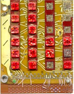
Fig. 6. Fragment of the computer board "Argon".
Part of the IP is dismantled for research
long-term effects
on them outer space.
Thanks to such a concentration of resources, the results of the Ministry of Electronprom, and first of all its SC, for many years looked good at the level of world microelectronics. Already the first product - the Micro radio - had no equal in the world. The first hybrid IPs corresponded to the world level [11]. By the way, the first IPs in the world to fly around the moon (in 1969) and return back were the Angstrom “Paths” (Fig. 6). In 1972, a new direction was mastered at NIIP - multilayer IS “Talisman”. The technology for creating these IPs then had no world analogues. It sharply reduced the size, increased the speed and reliability of the IP. In semiconductor ICs, at first we noticeably lagged behind, but soon caught up with world leaders. In the 1970s, Intel was the most successful semiconductor company. Compared with her, NIITT and Angstrom in the leading areas initially had some lag.
For example, Intel released 4Kbit dynamic RAM in 1974. - “Angstrom” in 1975, 16 Kbit - respectively in 1977 and the beginning of 1978, and both companies introduced 64 Kbit to the market almost simultaneously in 1979 [12].
A similar situation took place at the NIIME with the Micron plant. In the early 1970s, the director of NIIME K.A. Valiev, while in the United States at Motorola, showed the 500 Series IS (an analogue of Motorola's MSOOOO). After examining the samples, the specialists of the company stated: “Your circuits really have higher speed compared to the MC 10000, you have good technology” [13].
At the beginning of the five-year plan [1976], Americans wrote that in microelectronics we are 8 years behind them. And, one must think, rejoiced at this. However, by the end of the 70s, their joy, apparently, had diminished. Having studied several samples of our circuits in 1979, the Americans estimated this lag at 2-2.5 years . Transferred samples were taken from serial production. In the January issue of the American journal "Electronics" and he is very authoritative in this area, it is already noted, I quote: "The technological base and qualifications of technologists allow the Soviet Union to produce integrated circuits of almost the same quality as in the United States." And then a summary: “Probably, the schemes obtained do not reflect the highest technical level of the Soviet Union in this area. The integrated circuits used in the USSR for their own needs can be technically more advanced ”[8]. In the latter, they turned out to be right: the microprocessor ICs of the K587 series (developed in 1975) and 16 Kbit RAM (early 1978) were analyzed.
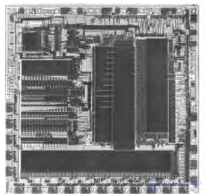
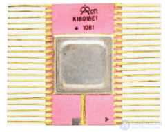
Fig. 7 K1801BE1 in the housing
(full size) and topology.
Photo by the author.
The culmination of this competition was 1979, when the NIITT developed a single-chip 16-bit computer K1801BE1 (Fig. 7) with the architecture "Electronics SC" (in the current terminology - a microcontroller). According to the conclusion of the interdepartmental state commission that adopted the development, such a computer abroad did not yet exist. On the whole, from 1964 to 1980, the lag of development in research centers for various types of IP compared to the foreign level ranged from zero to three years. Sometimes they pulled forward. But approximately the same dynamics was observed among leading foreign companies - they were either slightly behind the competitors, or ahead of them. Thus, it can be argued that the development of Zelenograd SC in those years as a whole corresponded to the world level. As a rule, his exits to international exhibitions caused surprise of foreign specialists and toughening of restrictions by CoCom. In general, “... in 1978-1980, domestic microelectronics, and especially the efforts of Zelenograd enterprises, was very close in its capabilities and results to the level that existed in the USA” [4]. The hardware development of the SC enterprises was also basically not inferior to the world level. The performance of the 5E53 modular supercomputer developed in DIC Yuditsky, surpassed everything known then in the world. Not inferior to its contemporaries the mini-computer “Electronics NTs-1” developed there was the same in G.I. Guskova: “... the equipment they developed exceeded the corresponding American counterparts” [4].
It should be noted that the original developments of IS and computers that did not have direct foreign analogues were competitive.
However, in terms of integrated circuit output, the Ministry of Electronics significantly lagged behind the foreign level. He did not satisfy the country's needs either - there were not enough funds for the development of production capacities of serial plants (and they are very expensive in microelectronics). As a result, the load on Zelenograd pilot plants increased sharply. “ The situation that arose when the experimental plants of the Scientific and Technical Center mostly turned out to be busy with serial production of integrated circuits began to adversely affect the future prospects of the development of microelectronics ” [14]. The possibilities of testing new materials, processes, technological routes, equipment and products at pilot plants were sharply limited.
Around 1980, a progressive lag began. There are many reasons for this, but the following can be attributed to the main ones:
Let us dwell on the last, purely internal reason — the radical change in the specialization of the Ministry of Electronprom, which contradicts its original purpose. This was publicly announced by the Minister of Economic Development, V.G. Kolesnikov at the end of the 80s at a meeting of the expanded Board of the IEP, in the preparation and conduct of which the author participated. The college was dedicated to the program for the development of microprocessor-based computer technology (MSWT): microprocessors, computers, peripherals and application systems. In his opening remarks, the Minister said: “ The Ministry of Electronics has three main areas: microelectronics, MWET and video technology . ” And these were not just words. Earlier, first as the First Deputy Minister, and since 1985, already in the role of Minister, V.G. Kolesnikov, in fact, headed for the transformation of the IET into the machine-building industry. A.I. Shokin also developed mechanical engineering and computer technology, but for the needs of the industry, not provided by specialized departments.
In fact, companies designing ICs, especially complex ones, such as microprocessors, are doomed to develop devices in which these ICs are used, such as computers. This is necessary, firstly, to develop and confirm the correctness of the IP project, and secondly, to create their primary market. But this does not require the organization of their own mass production of equipment, and the decree on the creation of a digital CM was supposed to transfer such projects to serial plants in the country.
But V.G. Kolesnikov began to compete with the Ministry of Radio Industry and the Ministry of Instrumentation in their field - the MEP produced more personal computers than all other departments together and the VCRs were released only in the MEP. V.G. Kolesnikov had powerful organizational skills. This talent would be, his energy would be - yes, for the development of microelectronics. But a significant part of the resources of both the minister and the ministry was aimed at creating a huge apparatus-making industry in the IEP: dozens of research institutes, design bureaus and factories that created and replicated MCWTs, video equipment, and household electronic equipment. And the necessary intelligence, human, material and financial resources were taken, of course, due to microelectronics. After all, the resources of the ministry were limited, they were sorely lacking for the development of the necessary capacities for serial production of microcircuits.
We give an example. In 1983, NIIP began work on dynamic RAM with a capacity of 1 Mbit. At that time there was a huge breakthrough and a huge potential market. The IP was developed, but there was nothing to produce it - the production required a technology of 1 micron level, but the available cleanrooms and equipment did not provide such accuracy then. Here is how the director of NIIP and the plant in 1981-1987 recalls A.T. Yakovlev: “ The first concerns about the pace of development that arose in 1983 ... turned into a circulation, which was sent to the first deputy minister of the Ministry of Economic Development [V.G. Kolesnikov]. However, it took the MEP leadership five years to come to a decision on the construction of a new plant. In 1988, construction began. It dragged on for many years ” [15].
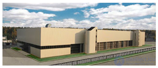
Fig. 8 New production building in Zelenograd. It seems that 15 years of expectations were not in vain -
in 2006, work on its development resumed. Photo by the author.
Thus, the leadership of the ministry did not respond to the timely question raised about the need to create a fundamentally new production with micron and submicron topological standards - there were not enough funds. But at that time in Zelenograd, non-core serial production plants were built for MEP - “ Kvant ” for personal computers and “ Elax ” - for magnetic disk drives. But there were no funds for new production for Mikron. A similar situation has developed in Voronezh (there was built a computer plant " Processor " ) and in other regions. As a result, the optimal moment for re-equipping the industry was missed, which led to a steady, ever-increasing lag. And the construction of a new production building focused on submicron technologies, begun in 1988 together with the German company Meissner & Wurst, was delayed - and again due to a lack of funds. Meanwhile, "the Germans undertook to build a turnkey plant in three years " [15]. In the end, it was built and equipped with all engineering equipment, but the reforms taking place in the country prevented the launch of the system. And it’s worth it, like a dumb reproach, a new technological module, ready to accept special equipment and begin mass production of modern ICs (Fig. 8).
After the minister’s change in 1985, the joke was popular at the Ministry of Electronics: “ We didn’t have time to recover from Shock when we got under the Wheel ” . But if " under Shock ", domestic microelectronics was created, rapidly developing and reached as a result of the world level, then " under the Wheel " it constantly lagged behind this level.

Comments
To leave a comment
History of computer technology and IT technology
Terms: History of computer technology and IT technology