Lecture
the development of microelectronic components is in the direction of increasing integration, performance and functionality. This process is characterized by an increase in the density of active elements on the chip by about 75% per year, which, in turn, necessitates an increase in the number of their leads on the package by 40% per year. It would seem that with an increase in the integration of microcircuits, the number of external interconnections and, accordingly, conclusions should decrease. However, the Rent rule, deduced long ago by an IBM engineer, is still valid for the developing element base:

where n is the number of microcircuit pins, k is the average number of interconnections per one logical element of the microcircuit ( k = 3 ... 4), N is the number of logical elements, R is the Rent ratio (for example, for processors R = 0.5 ... 0, 74).
Therefore, there is a growing demand for new packaging methods (pin designs), followed by an increase in PCB interconnect density. This is due to the desire to reduce the disintegration of active components during the transition to the next hierarchical level of interconnections in the equipment: a chip crystal, a microcircuit case, a mounting field for placing leads and connections on a printed circuit board, a printed circuit assembly (electronic module), an electronic unit, a system unit. At the level of the printed circuit assembly, the degree of disintegration can be characterized by the ratio of the areas of the crystal ( S 1), the case ( S 2) and the mounting field on the board ( S 3):
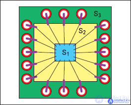
Figure: 1. Areas of the crystal (S1), the case (S2) and the mounting field on the board (S3)
For example, if the processor die has a size of 10 × 10 mm, and the mounting field of its case on the board occupies an area of 4000 mm2, such a design of the interconnection system is characterized by disintegration with the number 40. This figure estimates a matrix of 800 pins. The peripheral arrangement of such a number of leads with a pitch of 0.4 mm occupies a mounting field with an area of 10,000 mm2, which means that the degree of disintegration of such a design is 100.
It should be noted that the degree of disintegration grows as the hierarchical level of the structure increases: crystal - microcircuit - printed circuit assembly - module - block - ... For example, disintegration in a block can reach 100 thousand.
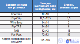
Table 1 shows the data of a rough estimate of disintegration when using various packaging methods and installing processor chips on a mounting base (board).
Table 1. Assessment of disintegration during the transition to the next level of interconnections
It is obvious that the degree of integration and disintegration must correspond to the technical level of production development. When trying to fulfill the design at the maximum production capabilities, the cost of the product will become unreasonably high due to the large volume of waste in the marriage. The reliability of such structures will also not be guaranteed. If, on the other hand, a product designed according to low design standards, that is, with a high degree of disintegration (large dimensions), goes into production, its high material consumption, low capital productivity ("from a cannon to sparrows") will no less detrimentally affect the prime cost.
But these ratios are only valid for microcircuits with the same level of integration. And since the processes of increasing the density of active components of microcircuits and increasing the density of the mounting field of microcircuit cases run in parallel, it is more fair to demonstrate the processes of increasing the mounting density by the number of pins placed on a certain area of the mounting field of the printed circuit board, as shown in Fig. 2.
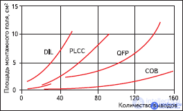
Figure: 2. The size of the mounting field to accommodate the pins of packages of various designs
In accordance with current trends, the area of mounting substrates is reduced by about 7%, and the physical dimensions of electronic equipment - by 10–20% per year. This trend is supported by the continuous increase in interconnect density by reducing mounting surfaces and increasing the number of leads. Subsequently, the connection elements, pitch and pin designs of components are reduced.
At the end of the 80s of the last century, a kind of revolution began in the production of electronics - the transition to surface mount technology. Then it seemed that the new technology will completely replace the installation of leads into holes. But it turned out that this is not always possible: large elements (high-capacity capacitors, connectors, transformers, etc.) are more convenient to mount with leads into holes. That is why the development of technology is not so much due to the displacement of components with pins for soldering into holes, but rather due to an increase in the proportion of surface mount components.
Until recently, the vast majority of package designs used a peripheral pinout. The development of packaging and mounting technologies for such components has reached its limit: the density of the arrangement of peripheral pins reaches a pitch of 0.4 mm (in rare cases, 0.3 mm). Therefore, in the 1990s, another revolution in editing technology began - the transition to a matrix of conclusions. In order to also increase the density of mounting in matrix cases, the pitch of the terminal grid is constantly decreasing: recently it was 1.0 mm, then it became 0.8 mm, now a step of 0.5 mm is maturing.
This is followed by a reduction in printed wiring elements: the width of conductors and gaps, holes and contact pads, the spatial (layer-by-layer) distribution of vias through the use of through, blind and blind holes. All this seriously affects the appearance of the assembly and assembly production: it is increasingly becoming automatic, many components cannot be manually installed or soldered. Accordingly, the cost of fixed assets of assembly and assembly production increases, but the volume of direct costs attributable to a single logic element of microcircuits decreases, and the production cycle is reduced. In turn, printed circuit boards, as well as mounting substrates for SMT components, become more complex and more expensive,but due to the increase in the functionality of electronic products, the cost of the functions they perform becomes ultimately lower.
Now there is a clear splicing of chips of microcircuits with a mounting substrate without intermediate mounting of a chip in a package, which should soon culminate in the creation of multichip module technology. In fact, its implementation is already possible today. But here the problems of heat removal arise: the higher the density of the crystals on the substrate, the higher the specific density of heat release - a consequence of the inevitable power dissipation. Without effective heat dissipation, the multichip module will simply overheat and burn out. Combining electrical and thermal structures in one mounting substrate is an urgent task in modern electronic design.
In fig. 3 demonstrates quite clearly the evolution and variety of packages and mounting substrates. This makes it possible to understand that today stable, all satisfying solutions have not yet been formed, from which a certain number of designs can be selected, thereby reducing the number of technologies required for their implementation.
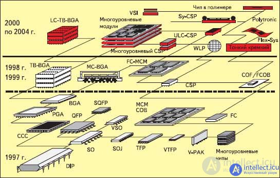
Figure: 3. Evolution of chip packages
From the very beginning, the chips of the microcircuits were placed inside ceramic or plastic cases. Until about 1986, all microcircuit cases had leads intended for installation in plated through-hole (PTH) of a printed circuit board and subsequent soldering. Later, with the increase in integration, conclusions began to be made in a form suitable for surface mounting technology (SMT - Surface Mounting Technology), a priority for the installation of electronic components.
At an intermediate stage in the development of mounting technologies, microcircuit cases have become widespread, suitable for both through hole and surface mounting.
The main types of microcircuit packages, depending on the location of their terminals (Fig. 4), are:
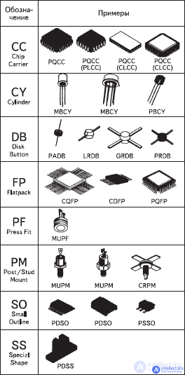
Figure: 4. Designation of structures of microcircuit cases
Most types of microcircuits have peripheral pinouts. The pitch of the peripheral pins is limited to 0.3 mm (practically - 0.4–0.5 mm), which allows microcircuits with large packages to have up to 500 pins. However, it should be taken into account that with a lead pitch of less than 0.5 mm, the output of suitable products decreases sharply, the strength of the contact nodes decreases, the likelihood of the appearance of solder bridges and injury to the insulating gaps between the leads increases. The variety of forms of conclusions is shown in Fig. five.
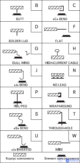
Figure: 5. Designation of pins of microcircuits
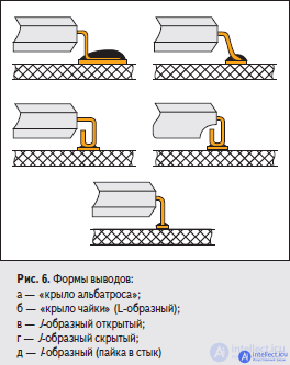
The most widespread are flat L- shaped leads such as "gull wing", "albatross wing", I- shaped and J- shaped leads, which compensate for thermal and mechanical deformations due to bending (Fig. 6).
The case with J- shaped leads (Fig. 7) takes up less space on the PCB, is stable during transportation, matches well with various packages, the cases do not get stuck in the feeders of the automatic devices for installing microcircuits on the PCB. The main disadvantage of these conclusions is the difficulty of visual inspection of the soldered joint .
Figure: 7. Package structure with J- pins
In the variant of molding with J -shaped hidden leads, it is possible to transfer the soldering point under the microcircuit case, due to which an arrangement with extremely small gaps between adjacent cases is possible. In addition, housings with a similar pin shape are able to fit into connector blocks, the contacts of which crimp the J- shaped pins of the case.
Housings with L- shaped leads (Figure 6b) are better controlled and standard probes are easy to use. With the automatic installation of ICs with the location of the leads on four sides, difficulties arise, since the cases get stuck in the transport paths and the leads are deformed. The main difference between the molding option with L- shaped leads ("gull wing") and the usual "albatross wing" is a significant reduction in the length of the soldered lead (to a size equal to or close to the width of the lead itself).
ICs in DIP packages (with I- shaped pins) were developed exclusively for mounting in holes, but due to the introduction of surface mounting technology, these chips are also adapted for surface mounting. Microcircuits with this form of leads can be mounted in the same way as microcircuits in packages with planar leads. In addition, ICs in DIP packages are surface-mounted by butt-soldering.
Most likely, in the future, the assembly of elements on printed circuit boards will be focused on soldering the leads under the casing of the elements using surface mount technology, and the lead pitch will be reduced. That is why electronic designers are interested in IC cases with a matrix pin arrangement such as BGA (Ball Grid Array).
Matrix components are very diverse (Figure 8):
Figure: 8. BGA packages
The matrix arrangement of contacts provides the highest packing density, the maximum number of contacts per case area (up to 700 contacts on a 35 × 35 mm case). The minimum transient capacities of the contacts (which ensures operability at higher clock rates of external data lines) are better in them than in other surface-mounted cases. In order for heat transfer to take place between the case and the printed circuit board, a special heat sink area is allocated in the center of the lower surface of the case.
It is assumed that microcircuits with the number of pins from 150 to 200 will be executed in packages with peripheral pins. For microcircuits with more than 150 ... 200 pins, a matrix pin system is preferable, since it makes it possible to place a large number of interconnects in a limited area.
Fuse Lead Designs in a Matrix System:
The matrix inference system provides obvious advantages , of which the most important are:
For solderless connection methods, for example, when using detachable connections, the body pins are made in the form of a matrix of contact pins mated with a matrix of sockets (Fig. The site https://intellect.icu. 9). Active and passive discrete components are placed on the surface free from contact pins in accordance with the circuit requirements. Heat dissipation is carried out from the upper surface of the case using a radiator and a fan, or, if it is a conductive heat sink, from special heat-dissipating elements connected to the heat-dissipating structures of the mounting substrate through a heat-conducting adhesive pad.
Figure: 9. Case with a matrix of contacts to be inserted into the socket of the connectors. Decoupling capacitors in the central area of the case
With a decrease in the lead pitch, it is especially important that the designers of printed circuit boards take into account the need to ensure the manufacturability of their designs, correctly assess not only the assembly, but also the production characteristics of the printed circuit boards from this point of view, so that the created designs guarantee the highest yield and the lowest cost of the finished product.
The need to reduce the mass and dimensions of electronic equipment structures has led to interest in methods of direct mounting of chips of microcircuits on a DCA (Direct Chip Attach) board: "chip-on-board" - COB (Chip-on-Board), "crystal-on-glass" - COG (Chip-on-Glass), "crystal-on-polymer" - COF (Chip-On-Flex) and, if there are many of them on the substrate, MCM (Multi-Chip-Module) "multichip modules".
Chip-on-Board (COB) technology locates chips directly on a PCB mounting surface. The crystal of the microcircuit is glued to the board and connected to it with thin wires, usually gold, with a diameter of about 25 microns. Then the entire structure is filled with a protective compound (Fig. 10).

Figure: 10. Mounting the crystal of the microcircuit directly on the board. Crystal-on-Board (COB) technology
The advantages of IDS are:
However, the comparatively large dimensions of the assembled PSI module do not allow using the experience of traditional technologies for mounting a crystal on a substrate. In particular, difficulties arise with the positioning of the crystal on the board and the alignment of the working elements of the tool with the pads for connecting wires on the crystal. Therefore, PCB technologies are beginning to be used to place crystals on a mounting substrate (Fig. 11).
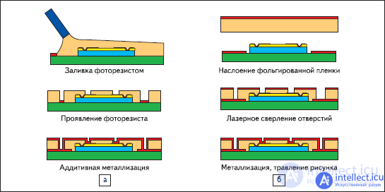
Figure: 11. Attachment of the contact points of the microcircuit crystal to the mounting substrate using the techniques of printed circuit boards: a) additive method, b) subtractive method
Crystal on polymer (COF) is an arrangement method in which a chip chip, passive and active components are arranged on a thin polyimide film. This technology provides a very small thickness and weight of the finished product, which is important when using such an assembly in compact devices (for example, in cell phones). The main disadvantages are the relatively high cost and low mechanical strength.
The crystal-on-glass design is preferred in display technologies, where the control chip, passive components, temperature compensation circuitry and character generator ROM are placed directly on the display substrate, which reduces the size and cost of the module. COG displays are widely used in portable devices. The disadvantage of this arrangement is the need for additional structural elements to protect against electromagnetic interference and infrared radiation.
Crystals of microcircuits are mounted on a substrate using one of four methods:
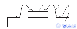
Fig. 12. Crystal layout by compression microwelding: 1 - microcircuit crystal, 2 - microwire, 3 - contact pad of the mounting substrate, 4 - substrate
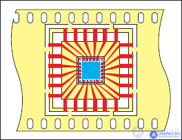
Figure: 13. Tape carrier of a chip of a microcircuit: 1 - a crystal of a microcircuit, 2 - a frame of a tape carrier, 3 - contact pads for mounting a carrier on a mounting substrate, 4 - a transport tape for automating the installation of a crystal on a mounting substrate
Figure: 14. Mounting the microcircuit on the substrate using the inverted crystal method: 1 - chip crystal, 2 - ball lead, 3 - contact pad of the mounting substrate

Figure: 15. Mounting the microcircuit using beam terminals: 1 - microcircuit crystal, 2 - beam terminal, 3 - contact pad of the mounting substrate
When assessing the possibility of using these methods, it is necessary to take into account the different temperature expansion coefficients of silicon crystals and a mounting substrate. This problem can be solved not only by choosing the appropriate substrate material. Another method is no less effective - pouring epoxy resin separating the die and the board. This technique makes it possible to equalize the deformations of the crystal and the substrate and, due to this, significantly improve the reliability of such assemblies.
When installing crystals on mounting substrates, it is not always possible to make sure in advance that they work correctly. To date, there are several technologies that eliminate this problem. By the way, in foreign companies there is a corresponding term - "knowingly good crystal" (KGD - Known Good Die). One of the ways to solve this problem is the use of microcases, the dimensions of which are only slightly larger than the dimensions of the crystal, but they perform the functions of protection from the external environment and redistribute the crystal leads to the matrix of the microclosure leads (Fig. 16). The use of microcases allows you to test the microcircuit before installing it on a mounting substrate. On microcircuits with programmable logic (FPGA), it is possible to program them by burning through the jumpers in accordance with a given scheme.A typical example of microcases is CSP (Chip-scale Packaging).
Figure: 16. Microcase CSP
Кремниевый кристалл стал ближе к печатной плате. Поскольку для некоторых CSP-корпусов шаг матричных выводов составляет 0,5 мм (0,020 дюйма) и менее, требуется использование специальных технологий производства печатных плат, позволяющих обеспечить разводку сигнальных цепей в узких пространствах между элементами монтажного поля. Уменьшение размеров элементов межсоединений приводит к значительным концентрациям механических напряжений, вызванных разницей в их коэффициентах теплового расширения. Из-за этого повысились требования к паяным соединениям, которые помимо обеспечения электрических соединений должны поглощать механическую нагрузку. При сокращении шага выводов до размера менее 0,8 мм происходит значительное уменьшение размера контактной площадки под пайку, что может привести к механической перегрузке и в конце концов к разрушению паяных соединений. Для решения этой проблемы разработаны новые способы подготовки поверхностей под пайку, обеспечившие большую стойкость паяных соединений.
Thanks to the existing technologies for the production of printed circuit boards, it is possible to mount the leads of open-frame microcircuits, if it is performed using thermocompression welding technology or using tape media (TAB technology). And although this solution transfers the difficulties of protecting open chips of microcircuits to the packaging of electronic modules, it is still one of the most effective methods for mounting chipless microcircuits.
When using packages with a small pitch of matrix leads, the situation is complicated by the fact that signal connections from the internal leads of the matrix must be brought out between the contact pads of the matrix. In this case, it is possible to draw one, maximum two conductors between the contact pads. Therefore, in most cases, the conductors from the internal pins of the matrix are led out along the inner layers of multilayer printed circuit boards.
Conventional through-hole multilayer PCB technologies are not capable of mounting ICs with matrix leads less than 1.0 mm (0.040 in.) Pitch. But there have already been created cases of microcircuits such as CSP with a matrix lead pitch of 0.508 mm (0.020 inches) and 0.254 mm (0.010 inches). For the installation of such components, special layers with blind metallized holes are added to the MPP, on which the wiring of circuits from under microcases or from under frameless microcircuit crystals is realized (Fig. 11).
These thin additional specialized layers are pressed onto the MPP, after which blind metallized holes are made in them. Abroad, this method is called SLC (Surface Laminar Circuit), which literally means "a circuit pressed onto the surface." Along with this, the term “built-up” is becoming more widespread. And although in Russia there is still no corresponding well-established concept, it is clear that the term built-up implies a combination of through-hole metallization and layer-by-layer build-up methods. This means that it can be given a long name - "MPP with layer-by-layer build-up of outer layers" or "MPP with blind holes" - until a more concise name is established among Russian specialists.
When choosing new packaging solutions, it should be borne in mind that the design of pins without an intermediate substrate, although it causes difficulties at the first stages of mastering this technology, ultimately turns out to be the most cost-effective option. As seen from Fig. 16, micro-package chip packaging has a high chance of becoming the basis for the layout of the future.
In this case, the package starts with a dielectric that connects the semiconductor through micro-junctions to a layer formed on top of which solder balls are located, which make it possible to create connections to the PCB during reflow soldering. Moreover, there is no need for an intermediate organic carrier, since the carrier is the silicon crystal itself, and the wire connections are replaced by a reliable technology for creating interconnections with a layer formed on top.
Until recently, this type of CSP was used relatively rarely. The reason, obviously, is not in the cost of packaging, but in the insufficiently developed technology of forming interconnections.
This means that with the proliferation of such packages, PCB design codes will be seriously revised and new types of interconnects in the Z-axis will be used. The requirements for soldering technology are also extremely stringent as the size of each solder joint on the PCB is significantly reduced.
Further prospects for the development of packaging technology are associated with the development of a multi-level (stack), or modular, technology, which is designed to reduce the density of interconnections outside the packages by using the concept of transferring interconnects inside a multi-chip module. For this, two-storey (Fig. 17), three-storey structures on rigid foundations are already used (Fig. 18). Flexible multilayer substrates allow reducing the mounting area of multichip modules (Fig. 19) by rolling them into a cubic shape (Fig. 20).
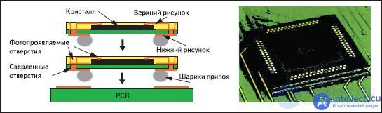
Figure: 17. Double-deck assembly of crystals or microcases
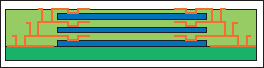
Figure: 18. Three-storey stacking of microcases

Figure: 19. Multi-chip module on flexible basis
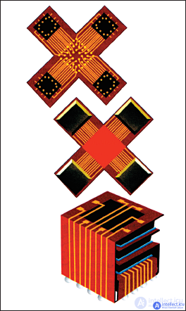
Figure: 20. Stacking a multichip module on a flexible mounting substrate
The element base for surface mounting includes an extensive range of discrete (loose) elements for various purposes. The simplest and most common type of package is rectangular, or chip (Chip). Almost all capacitors and resistors have a rectangular case with metal contacts on the sides (Fig. 21).
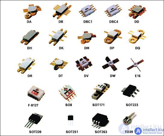
Figure: 21. Discrete Chip Components
Foreign manufacturers offer a wider range of chip elements. In addition to capacitors and resistors, there are inductors, electrolytic capacitors, diodes, zener diodes, switches and other elements.
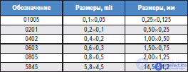
In the mil system, most of the chip components are designated by size in such a way that the first two digits indicate the length of the component in mil fractions, and the last two - the width (Table 2).
Table 2. Dimensions of chip components in the mil system
Another mass body type is cylindrical, or MELF (Metal ELectrode Facebonding) and MiniMELF. These cases have a glass case and metal contacts at the ends. Resistors and diodes are mounted in such cases.
The SOD (Small Outline Device) type package has been specially developed for diodes, which is a glass case with a metal cover. In order to distinguish the cathode from the anode placed in such housings, a black ring is applied to the glass case closer to the cathode.
The SOT (Small Outline Transistor) package is specially designed for transistors. Housings of this type have a plastic housing and metal leads on the sides.
Not only transistors and diodes are placed in SOT cases, but also transistors with resistors, zener diodes, voltage stabilizers based on an operational amplifier, and much more, and the number of pins can be more than three.
The general tendencies towards microminiaturization are associated with the huge costs of updating fixed assets in microelectronics, printed circuit boards and assembly and assembly production. Nevertheless, these tendencies manifest themselves in a variety of methods for increasing the density of interconnections in microcircuit packages, printed circuit boards, and assembly and assembly. In fig. 22. shows what methods of microminiaturization are used by various manufacturers of the element base, and in fig. Figure 23 shows the comparative cost of these techniques.
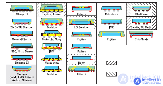
Figure: 22. Methods of microminiaturization of various firms
Figure: 23. Comparison of the cost of microcircuits microminiaturization methods
As for the passive components, they are reduced to the size of poppy grains: they are already moving from 0201 to 01005. But the transfer of passive components in the design of printed circuit boards is considered more fruitful: for one screen printing, for example, resistors can be applied, after another - a dielectric layer of capacitors ... However, discrete components are inevitably used when accurate resistor values or large capacitors are required.
Components are the weakest link in assembly soldering. This is especially true for lead-free soldering. The entire mass of components still in circulation on the market is intended for soldering with SnPb solders. On July 1, 2006, the RoHS directive came into force, prescribing the use of lead-free soldering technologies [11]. The first lead-free soldering components went on sale in 2000. They had the following solder coatings - Sn, SnCu and SnBi. But for lead-free soldering, there are still no coating standards for components, so firms that produce individual batches of components for lead-free soldering act at their own peril and risk.
There are several types of components that react differently to soldering conditions depending on the design:
Current leading component coatings:
The SnPb coating is completely incompatible with lead-free soldering. In general, we have to talk about the compatibility of solders of different systems when the components have SnPb - coating, and are used in lead-free processes. This alignment becomes a source of defects. This is especially true for components such as BGA and QFP. Some coatings, such as SnPbBi (90 ° C), SnBi (138 ° C), SnPbAg (179 ° C) and SnPb (183 ° C), reduce the melting point. But they create a risk in the management of the lead-free soldering process and reduce its reliability. The risk of soldering out of control is also increased when components are lead-free and soldered with SnPb solder. This gives rise to the possibility of delamination of the soldering and splashing of low-melting solder.
Pure tin solders well over a wide temperature range. However, its use is dangerous due to the possibility of recrystallization at temperatures below 13 ° C ("tin plague") and the formation of whiskers. But after soldering, pure tin ceases to be such, and therefore these fears are unjustified.
SnBi . Eutectic alloy 42Sn58Bi has a melting point of 138 ° C. A similar alloy, but containing 3% bismuth, melts at a temperature of 215–220 ° C. These alloys also exhibit whisker properties and, when combined with SnPb solders, this hazard does not disappear after soldering.
SnAg . These alloys exhibit good solderability and good mechanical properties, but they are expensive. Sn3.5Ag alloy is relatively cheap but tends to form whiskers. The Sn5.0Ag alloy is free of this drawback, but is more expensive and has an unacceptably high melting point.
NiPd was adopted by Texas Instruments in 1989. Since then, the company has sold millions of components with this coating and has no complaints.
SnCu . The eutectic Sn0.7Cu alloy is a relatively inexpensive, fine-grained solder alloy that exhibits good solderability. But he also shows a tendency to recrystallization of tin and the formation of whiskers. Melts at a temperature of 227 ° C.
High soldering temperatures lead to the need to require components to successfully pass thermal shock tests, which occurs when immersed in solder for 10 s at 260 ° C or for 5 s at 280 ° C. Housings must not explode (popcorn effect), deform, discolor or melt. Plastics with high heat resistance are more expensive than the previous ones used for SnPb brazing and adsorbing moisture. The amount of absorbed moisture depends on the hygroscopicity of the material and the design of the case. The absorbed moisture quickly turns into steam when heated. Steam pressure causes swelling (popcorn effect), tears, cracks. Even if the plastics do not crack, they can delaminate inside the case. Diffusion of moisture into the volume of the compound is proportional to the temperature and relative humidity of the environment.The lower the volume of the body, the earlier the complete equilibrium with the external environment occurs.
Thermal shock testing of components is carried out in three stages:
There are regulations [12] that define the temperature and humidity levels, after which the component housings must withstand thermal shock. Subsequently, these levels correlate with the permitted residence time of unpacked components in a controlled environment of the workshop before entering the assembly line, which can range from 4 to 24 hours. If during this time the components do not go to soldering, they must be stored in dry cabinets where the relative humidity is maintained at 3-5%.
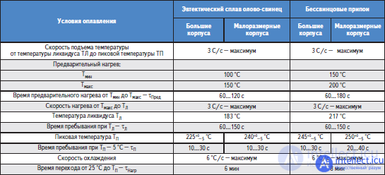
Table 3 shows test conditions that simulate reflow soldering conditions with eutectic tin-lead and lead-free alloys. The soldering temperature profile (Fig. 24) shows the symbols used in Table 3.
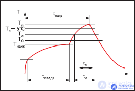
Figure: 24. Soldering temperature profile
Table 3. Test modes for heating components simulating reflow soldering conditions (comparison of soldering modes with tin, lead and lead-free solders)
Regardless of the fact that printed circuit boards belong to the independent production of mounting substrates, they can be attributed to the components of the assembly and installation production, as products coming from outside. Therefore, there is no need to consider PCB technology. Corresponding publications [1–5] and numerous publications in popular journals [6–10] are devoted to them.
Here it makes sense to consider the issues of interfacing of modern components with printed circuit boards that act as mounting substrates.
PCB Requirements
What should we be interested in about printed circuit boards in relation to the requirements of assembly and assembly production?
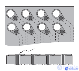
Figure: 25. One way to prevent the flow of molten solder into the hole
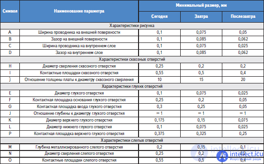
The designation of the geometric characteristics of printed circuit boards is shown in Fig. 26, and the numerical characteristics of the boards (today and in the future) are shown in Table 4.
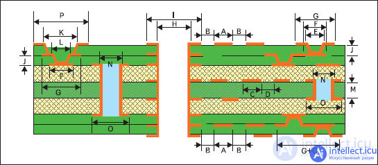
Figure: 26. Geometric characteristics of the MPP
Table 4. Numerical characteristics of the MPP
Mounting base materials
To avoid the problems of delamination and warping of PCB bases, they must be made of materials with a higher glass transition temperature ( Tg ) - about 150 ° C and higher. The group of materials such as FR-41 with Tg = 125 ° C, usually used for soldering with SnPb alloy, is no longer suitable for soldering with SnAgCu alloy. The behavior of the base material is especially critical during the HASL hot service. Materials like FR-52 and polyimide boards can be used for lead-free soldering without restriction. Cheap materials like FR-1, FR-2, FR-3 with Tg <130 ° С are no longer suitable for lead-free soldering.
1 FR - Fire Restardent (fire resistant). FR-4 is a glass fiber reinforced epoxy resin. FR-1 = FR-2 - phenol-formaldehyde-impregnated paper. FR-3 is an epoxy impregnated paper.
2 FR-5 is a multifunctional epoxy resin (Tg = 150… 160 ° С), reinforced with high-grade fiberglass.
RoHS (Restriction of the use of certain Hazardous Substances in electrical and electronic equipment) laws propose moving away from halogen flame arresters, which are part of the PCB bonding material. FR-4 materials with such a binder have a Tg in the 130–150 ° C range, which is acceptable for lead-free soldering. But the cost of such materials is more than 30% higher. To reduce the cost, cellulose (CEM-1) or glass (CEM-3) paper (CEM - Composite Epoxy Material) is introduced into the composition of the reinforcing components. Such materials are softer for drilling, when they are used, the walls of the holes are smoother, and the drill consumption is less, which creates some advantages for them over FR-4.
Hole plating
The ductility of the copper deposits should be related to the thermal expansion of the base of the boards along the Z-axis. It will be clearly greater at higher soldering temperatures with lead-free solders. To resist expansion of the base and to ensure greater strength and ductility of copper deposits, it is necessary to tighter control of the process of metallization of through holes. To ensure the heating of the through mounting holes to the higher temperatures inherent in lead-free soldering, it is necessary to ensure the appropriate thermal conductivity of the metallization by increasing its thickness. The above makes it necessary to revise the requirements for the technology of metallization of holes in printed circuit boards.
Solder coatings
A wide variety of topcoats indicates that there is no choice in favor of any one or two that meet all the requirements for cost, wettability, durability, etc. Their list is wide:
In this series, OSP, ENIG, ImAg and HALS are the leading PCB coatings for lead-free soldering [2, 4].
The HASL process of hot tinplate plating consists in immersing them for a limited time in a bath of molten solder. During quick removal of the boards, they are blown with a jet of hot air, which blows off excess solder and levels the coating. But despite the efforts, the beads of solder remain. There are especially many of them on developed metal surfaces. In subsequent assembly, sagging interferes with the placement of small components, which limits the use of HASL. However, in terms of quality and exceptional solderability, this coating is by far the best. Therefore, where PCB manufacturing and assembly takes place in the same production, they always try to find compromises in order to use HASL.
Another significant drawback of the HASL process is the hard thermal shock that boards experience when immersed in molten solder. The higher the working temperature of the solder, the more serious the problem of ensuring the reliability of the interconnects. A number of enterprises do not use HASL processes for multilayer boards, believing that they reduce the reliability of internal interconnections due to such thermal shock. There are currently no lead-free solders of acceptable quality and relatively low temperature for HASL processes.
The OSP coating protects the copper surface from oxidation during storage and soldering. At the end of soldering, such a layer, having fulfilled its function, loses the ability to provide subsequent soldering processes. This cheap coating has been in use in Japan for over 20 years. But in order for the soldering process to take place in one stage of group heating, product designers take this feature into account in order to reduce the cost. OSP is a good alternative to HASL. However, OSP has a short life cycle, which negatively affects technological reliability. This coating does not provide multiple soldering, especially at high temperatures. To avoid such difficulties, it is necessary to use nitrogen as a neutral soldering medium.
ENIG coverage(~ 4 μm Ni + ~ 0.1 μm Au) is another alternative to HASL processes. This coating is free from ionic contamination and is capable of being re-soldered at high temperatures. A thin layer of gold protects nickel from oxidation, and nickel becomes a barrier preventing the mutual diffusion of gold and copper. A typical defect for ENIG plating is the black pads that appear on the surface due to the release of nickel and reduced phosphorus. During soldering, gold dissolves in the solder and exposes a poorly soldered phosphorus layer. The solder rolls off the phosphorized surface, which is why the black pad effect appears. Black contact pads can also occur if the soldering process is overexposed. Overexposure intensifies the formation of intermetallic compounds of tin with nickel and tin with phosphorus embedded in nickel.The release of phosphorus on the nickel surface can also trigger the gilding process. The precipitation of gold from neutral electrolytes reduces the likelihood of these phenomena [13].
ENIG is capricious in its choice of fluxes, and its price is about 25% higher than that of OSP. ENIG advantages:
Immersion tin (ImmSn) is another alternative to HASL processes. The popularity of ImmSn is growing due to its good wettability and ease of deposition. ImmSn exhibits better solderability than ENIG.
There are limitations for using ImmSn:
But ImmSn also has advantages:
Immersion silver (ImmAg) . The ImmAg thickness does not exceed 200 nm, so the cost of implementing this coating is insignificant. The viability of ImmAg is much higher than OSP, but slightly less than ENIG. Changes in the color of the coating during storage, assembly and soldering are the result of air pollution with sulfates and chlorides. Yellowing does not affect the properties of ImmAg, but the decorative effect of the coating suffers. Antioxidant preservative coatings inhibit the yellowing process and prolong the life of the coating. ImmAg is less popular in Europe than in the US, where it is more readily available [14].
Continuous integration of the element base, reduction in the size of passive components prompts the development of interconnection technology (printed circuit boards, connectors, switching elements) and technology for assembling and mounting components on mounting substrates. New technologies related to the implementation of the RoHS Directive are aggressively intervening in this direction of development of electronics. Traditionally established approaches and design methods and technologies for their implementation need to be revised so that they remain at the same level of reliability as it was before the transition to lead-free technologies. From this point of view, things can come to the point of abandoning the use of individual case designs (such as BGAs and the like) in highly reliable systems, if they are intended for lead-free soldering.

Comments
To leave a comment
History of computer technology and IT technology
Terms: History of computer technology and IT technology