Lecture
TSMC and Matrix Semiconductor, the world's first commercial model of a three-dimensional semiconductor device Matrix 3-D Memory, were presented at the end of 2001. I must say that universities, research laboratories and individual scientists have attempted to create three-dimensional integrated circuits since the beginning of 70 years of the last century. In addition to the use of polycrystalline silicon, the change in the structure of which was supposed to be carried out with the help of a laser beam, other constructive solutions were envisaged in these works, allowing to place several two-dimensional microcircuits one above the other.
Generally speaking, for those applications where the situation is caused by the ever increasing reduction in the size of microcircuits and the reduction in the cost of their development, the three-dimensional architecture of semiconductor devices would achieve striking advantages in price as compared to traditional ones. Modern integrated circuits are two-dimensional (often referred to as "planar") for one simple reason. The fact is that the quality of crystals, which is necessary for creating the best transistors, is preserved only in the substrate or in the silicon base itself. As soon as an insulating oxide or a binder metal is applied to this substrate, it becomes impossible to sequentially place the silicon atoms so that they form the desired crystal lattice. The required substrate pattern is hidden under these layers. As a result, traditional transistors are created only in the top layer of the silicon substrate, and the space above the base is used only for interconnects. Nevertheless, the main motivation for the transition to a three-dimensional architecture is very simple. As in the case of real estate, the cost of silicon directly depends on the size of the used area (and not on the volume). Thus, the three-dimensional method of production has two obvious advantages. Firstly, this is a significant reduction in prices per fixed device and, secondly, an increase in the number of transistors per chip at a rate not lower than that provided by Moore’s law in terms of the number of devices per unit area.
Since the structure of a three-dimensional integrated circuit is based on a two-dimensional architecture (construction of real devices, and not just insulators and interconnects on a circuit above the substrate), the three-dimensional circuit can use all existing advances in semiconductor devices, and in addition to create a completely updated range of solutions. Experts believe that a radical increase in the density, which becomes possible due to the vertical placement of elements, will quite realistically contribute to a multiple reduction in the cost of manufacturing microcircuits compared to traditional microcircuits with the same production technology. Interestingly, according to one estimate, making an acre of conventional silicon transistors costs about a billion dollars.
In addition, experts quite reasonably assume that 3D chips could scale at least as fast as Moore’s law provides, thereby giving consumers the ability to use all the advantages of 3D technology over time and still reduce production costs, on which count industry participants.
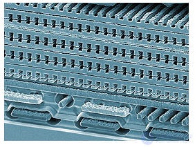
Crystal Matrix 3-D Memory contains four transistor layers
In 1998, two professors at Stanford University, Mark Johnson and Thomas Lee, were at the head of the new company MatrixSemiconductor, which started creating three-dimensional (3D) semiconductor devices. The latter began his career as a chip designer as far back as Analog Devices. In 1992, Thomas Lee joined Rambus, where he developed high-speed RAM microchips using CMOS technology. In addition, he was involved in the creation of some microprocessors, in particular K6 and K7, in Advanced Micro Devices, as well as StrongARM and Alpha processors in Digital Equipment. In 1994, Professor Lee was invited to Stanford University, where his main research interests were focused on microcircuits, both wired and wireless, in the gigahertz range.
The basis of the projected products of the newly formed company lay the technology of multi-layered transistors. Today, Matrix Semiconductor’s investors include such major corporations as Nintendo, Microsoft, Seagate, Sony and Thomson. I must say that the very idea of 3D transistors experienced ups and downs. At first, Matrix Semiconductor planned to start mass production of its microchips in 2002. However, according to one of the leading managers of the company, the main lesson learned from the subsequent failures was that it was easy to make something in one copy, but to produce the same in millions of copies very hard. The design of the chip and the process of their manufacture had to make major changes.
Despite a series of delays, Matrix Semiconductor in the summer of 2004 still released three-dimensional memory chips using the power of the Taiwan semiconductor giant TSMC. In the production of crystals to obtain the base layers, design standards of 0.15 microns are observed, and for subsequent ones - 0.13 microns. Unlike flash memory, Matrix 3-D Memory chips are write-once ROMs. In other words, the data is recorded on them by the method of "burning" fusible jumpers. For this reason, the potential market for them is rather narrow. However, it should be noted that the cost of such products is almost half that of flash memory. Therefore, the company is primarily aimed at industrial customers who want to produce crystals with recordings of audio, video and other immutable files. For example, the company Mattel has adapted this crystal for storing cartoons on its portable video player JuiceBox. Another potential customer is Nintendo Corporation. Back in early 2003, this gaming giant invested about $ 15 million in Matrix Semiconductor.
The company paid particular attention to compatibility with current standards - new non-volatile memory microcircuits are compatible with NAND flash contacts with flash memory chips. Thanks to this, Matrix 3-D Memory cards can be inserted into slots for flash media of various digital devices (including cameras, players, handheld gaming consoles, personal electronic secretaries, mobile phones, etc.), using them as an inexpensive alternative to write once information.
In early May of this year, Matrix Semiconductor announced a new crystal of three-dimensional memory (having four levels of transistors) with a capacity of 1 Gbit and a size of only 31 square meters. mm
"3D" transistors
Around the same time, when the triumphant reports about the creation of three-dimensional semiconductors came from Matrix Semiconductor, scientists from IBM Research - the research division of IBM - at the International Conference on Circuit Design of the International Electron Devices Meeting told about the new design of three-dimensional microchips in which transistors are located in two or more layers, and the manufacturing process resembles baking a multi-layer cake. In their opinion, over time, such a design can lead to the emergence of more powerful microprocessors with a much larger number of transistors compared with modern single-layer structures. In addition, in this case the length of the conductors connecting the transistors in the microcircuit is reduced. Today, experts say that the approaches used by researchers from MatrixSemiconductor and IBM were quite close, but at IBM, they more realistically looked at things and evaluated the new technology only as promising.
It should be noted that at the beginning of the 21st century many major corporations began to show interest in semiconductor devices with a three-dimensional structure. So, IBM researchers in 2001 announced the creation of an alternative type of transistor, which, thanks to better control of the short channel effect, sub-threshold voltage characteristic close to ideal, and high carrier mobility in the channel, could become a promising candidate for future high-density chips low power consumption. When developing this device, the corporation’s experience in silicon-on-insulator technology proved invaluable. The transistor current with two gates and, therefore, its signal is almost twice as high as in a conventional MOS device with large element sizes. Such a structure is easy to scale, and on its base you can perform almost any type of MOSFET. The main task in its formation is to obtain an acceptable value of the threshold voltage of transistors of high-speed logic devices while monitoring the channel conductivity value.
Of particular interest is a type of double-gate transistor –FinFET. In this device, a thin silicon body (column, inset - fin) is as if wrapped by a gate, which forms two aligned channels located on both sides of the silicon body. The protruding front region of the body is the source of the transistor, the protruding rear region is the drain. The current flows in a plane parallel to the plane of the body, i.e., although the gates protrude beyond this plane, the FinFET structure can be regarded as quasi-planar. The active width of the device is equal to the height of the body column, and it can be increased by parallel inclusion of many columns. In its topology, FinFET does not differ from the traditional MOS transistor, except that the active region is formed by inserts, and does not constitute a flat rectangle. FinFET manufacturing is easy to set up: all the necessary technological operations are widely used in modern semiconductor manufacturing and are well developed. True, the most critical parameter of this structure — the thickness of the channel — depends on the resolution of the lithography process.
IBM has created symmetric and asymmetric n-and p-channel MOS transistors of this type, the characteristics of which are optimized to obtain high speed and low threshold voltage, respectively. The process of manufacturing a fully depleted symmetric FinFET involves the formation of a body-insert with a thickness of 20 nm by photolithography methods. The gate structure consists of a thermally grown oxynitride film 1.6 nm thick and polycrystalline silicon. The protruding source / drain areas are fabricated by conducting ion implantation on four sides of the plate.
Together, the University of California at Berkeley, Intel Corporation and the Lawrence National Laboratory created a FinFET structure with a channel length of less than 20 nm, in which the size of the silicon insert is given by the gaps between the polysilicon gates, and the source / drain area - the lithography process. Due to the application of special films on the side walls of each intermediate gap, the developers managed to double the current of the transistor and reduce the insert thickness in comparison with devices made using only the lithography process. The gate structure consisted of a thermally grown oxide 2.4 nm thick and SiGe 400 nm thick.
AMD's new FinFET transistor is the result of its collaboration with scientists at the University of California and the Semiconductor Research consortium. This device had a gate length of only 10 nm.
Transistors for "Platform 2015"
As you know, Intel’s long-term vision of developing the fundamental elements of the platforms, as well as architectural innovations and fundamental knowledge that drive this development, are set forth by analysts in the Platform 2015 document. There, in particular, it is said that by 2015 and further, semiconductor production CMOS technology will develop at the same pace as now. The trend of new materials and new structures will continue. In addition, High-K / Metal Gate insulators and three-dimensional gate transistors (or Tri-Gate transistors) are named as examples of technologies that are under development.

Tri-Gate - a three-dimensional gate transistor
As it is known, the experimental design of the transistor, called Tri-Gate, was first introduced in Japan at the International Solid State Device and Materials conference in 2002. It was based on a three-dimensional structure consisting of a “microbar,” which from three sides fit an insulator and a conductor shutter. Such a structure allowed sending electrical signals both on the upper part of the “bar” and on both its vertical sides. "Microbar" turns into a source (drain) outside the gate. The area thus increased, which is available for signal transmission, makes it possible to pass 20% more current compared to a traditional planar structure occupying a similar area.
The Tri-Gate uses elements of the TeraHertz technology, presented by Intel experts in December 2001. This technology allows the creation of transistors that operate at switching frequencies of the order of terahertz and are capable of scaling. This class of transistors is designed to maximize the level of performance while reducing power consumption and cost of production. Note that transistors made on the basis of High-k / Metal Gate and Tri-Gate technologies belong to TeraHertz class.
The triple gate is built on a superfine layer of fully depleted silicon, which reduces the leakage current of a closed transistor. It has an accumulated drain and source, allowing to avoid an increase in resistance with a decrease in the size of the transistor. In addition, a high K dielectric can be used in the new transistor, further reducing the gate leakage current.
Recall that the presence of a thin layer of dioxide is necessary to achieve high performance characteristics of the gate dielectric. Silicon dioxide is a material whose molecules consist of one silicon atom and two oxygen atoms. It is a good insulator, but the problem is that the thinner the silica layer, the higher the leakage current passing through the insulator. Consequently, it was necessary to replace silicon dioxide with new materials with the same properties, the use of which does not require achieving a low layer thickness.
The material based on High-k technology is able to replace silicon dioxide in the manufacture of the gate electrode, since this material has very good insulating properties and also creates sufficient capacitance between the gate and the channel. Both of these properties are desirable to achieve high performance transistors. The symbol "k" (in fact, the Greek letter "kappa") indicates the ability of a material to maintain an electric charge. Those materials that can store electrical charge better than others have a higher "k" value. The use of materials based on High-Technology technology reduces leakage, since these materials may have a different thickness than silicon dioxide, while maintaining the same properties.
Another advantage of the Tri-Gate transistors is that it is possible to produce chips based on them using existing equipment. In addition, structures can be built from several Tri-Gate bars to form power transistors. As noted by Intel, this type of transistor was developed by the corporation to enable the deployment of a new 45-nanometer process technology in 2007. Also, Intel plans more in-depth research in the field of III-V transistors, carbon nanotubes and silicon nanowires. The goal of all these studies is to increase the speed of the devices, further reduce their size, power management and reduction of power consumption. In addition, the integration between the architecture of crystals and production technology will achieve even greater density: billions of transistors can be located on a single crystal. This approach is very important. In the process of creating microprocessors and platforms of the future, developers and technologists should cooperate very closely.

Comments
To leave a comment
History of computer technology and IT technology
Terms: History of computer technology and IT technology