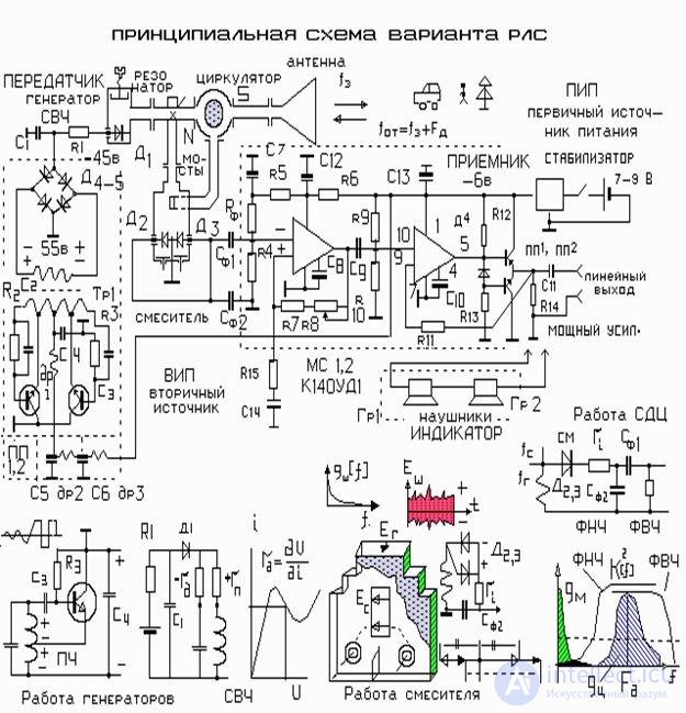
Transmitter
The transmitter is assembled on avalanche-span diode LPD D 1 . Power supply requires 50 V 10 ma. The primary power source has a voltage of 7-9 V. Therefore, the secondary source is built according to a circuit with an increase in voltage. Voltage 7-9 V is applied to a square wave generator. It is assembled on transistors according to the scheme of a two-stroke generator operating at a frequency of 500 kHz on a miniature transformer with an annular ferrite core. From the step-up winding of the transformer, an alternating voltage of 60 V enters the diode bridge D 4 -D 5 . The rectified voltage is filtered with capacitance C 1 and through resistor R 1 is fed to the LPD.
Antenna-feeder path
From the LPD camera, the probing signal goes to the circulator and from there to the antenna. On the way, part of the power is diverted through a coupler to a balanced mixer.
The reflected signal from the antenna through the circulator is sent to the mixer.
Mixer
The tension of the local oscillator is removed from the coupler and fed to the in-phase two-shoulder microwave bridge, and from each arm to the mixing diodes D 2 -D 3 . The diodes are turned on in antiphase, so the detected local oscillator noise at the load R 4 - C f1 C f2 have different polarity and are compensated. The noise compensation is incomplete , since the transmission coefficients of the mixer arms cannot be performed with absolute precision.
The reflected signal arrives in the middle of the bridge using a waveguide deployed across. Due to this, the reflected signal falls on the mixing diodes in antiphase. And since the diodes are antiphase, common-mode addition occurs on the load. The voltage of the reflected signal is doubled and is received at the input of the receiver. Vector diagrams and principles of operation are explained in the figure below the diagram.
Receiver
The receiver is built according to the low-frequency amplifier circuit on MS 12 operational amplifiers .
For powering a unipolar voltage of the battery used voltage dividers for resistors R 4 - R f - R 9 R 10 . Chips work with feedback on resistors R 7,8,15 - R 11 . The output stage of the receiver is designed to work on headphones. It is filled according to the scheme of emitter followers on transistors PP 1 -PP 2 and covered by negative feedback.
Filters
In the low pass filter works according to the scheme of the integrating RC link. Used internally resistance mixing diodes and capacitance C f2 . The upper cutoff of the filter is tuned to a frequency of 5 kHz. Due to this, the noise spectrum with frequencies above 5-7 kHz is suppressed.
Filter SCC is built according to the scheme of the high-pass filter on R f1 -C f . The frequency of the lower cut filter is 30-40 Hz. Due to this, the terrain spectrum lying in the region of 5–20 Hz is suppressed, and the spectra of signals from moving targets “pass” to the receiver.

Comments
To leave a comment
Radio Engineering Systems
Terms: Radio Engineering Systems