Lecture
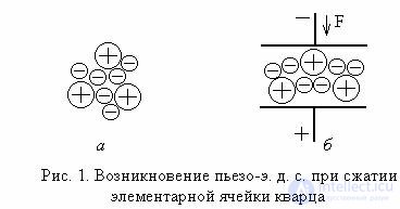
In fig. 1, a shows the structure of a quartz elementary cell consisting of 3x silica molecules. In the absence of deformation, the center of gravity of the positive and negative ions coincides (silicon ions are noted with a plus, oxygen is a minus). Compression of the crystal in the vertical direction (Fig. 1, b) leads to the displacement of positive ions downwards and negative ones upwards. Accordingly, a potential difference appears on the outer electrodes. The considered phenomenon is called the direct piezoelectric effect. There is also a reverse piezoelectric effect, when, under the action of the applied voltage and depending on its polarity, the piezocrystal (quartz, Rochelle salt, tourmaline, etc.) is polarized and changes its geometric dimensions. If an alternating voltage is applied to a piezocrystal, then mechanical oscillations of a certain frequency, depending on the size of the crystal, are excited in it. The phenomena of direct and inverse piezoelectric effect have been known for a long time. However, only in recent years, thanks to the development of semiconductor technology and microelectronics, has it been possible to create qualitatively new acoustoelectronic functional devices.
In 1956, K. B. Tolpygo and Z.I. Uritsky [9] and, independently, G. Weinreich [10], suggested the possibility of amplification of OAB by supersonic drift electron flow. This effect was first discovered and studied experimentally in 1961. А.Р. Hatson, J.G. McPhee and D.L. White [11] in the piezoelectric semiconductor CdS. The gain obtained was quite large; for example, at a frequency of 45 MHz, it was 54 dB * cm-1.
In view of the emerging fundamental possibility of creating new types of semiconductor amplifiers and generators, this work caused a torrential flow of research on acoustoelectronic phenomena in solids. piezoelectric, non-piezoelectric, multi-valley, with "hot" electrons, magnetic, etc.
It has been shown that the AV gain mechanism in the “low frequency” case,
kl <1,
where k is the wave number AB, l is the mean free path of electrons, is similar to the amplification mechanism in a traveling-wave tube (TWT). The piezoelectric field AB collects electrons into bunches, which, moving along with the wave, turn out to be either in the rear (Fig. 2a) or in the front (Fig. 2b) slope of the potential wells created by AB, depending on the electron drift velocity Vd. In the first case (Fig. 2a), Vd <FAB, AB is absorbed and damped, in the second (Fig. 2b), Vd> FAB, amplifies4 (VAB is the speed AB).

Fig. 2. Amplification of acoustic waves in semiconductors by supersonic electron drift: (a) Vd <VАВ - “electronic” absorption; (b) Vd> VAB - “electronic gain”.

Comments
To leave a comment
Acoustoelectronics and acoustooptics
Terms: Acoustoelectronics and acoustooptics