Lecture
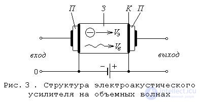
One of the main devices of acoustoelectronics, whose action is based on the phenomenon considered, is an electroacoustic amplifier (EIA). In fig. 3 shows a diagram of such an amplifier in bulk waves. At the ends of the semiconductor Zvukovaya (Z) are located piezoelectric transducers (P), which are connected with the ohmic contacts (K) from one side to the sound conduit, and from the other to the input and output terminals. When an alternating voltage is applied to the input, an acoustic wave is excited in the input piezoelectric transducer, which propagates through the acoustic conductor. The interaction of the wave with electrons moving in the same direction along the semiconductor acoustic conductor ensures its amplification. Consider this phenomenon. Suppose that a harmonic longitudinal acoustic wave is introduced into the sound duct, moving at a speed Vb. The pressure in the crystal varies from point to point. In those places where the crystal is compressed, the piezo - emf. slows down the movement of electrons, and in those places where it is stretched - accelerates. As a result of this, at the beginning of each period of the wave, electron bunches form. When Ve> Vb, the bunches move in the decelerating parts of the wave and transfer their energy to it, which is what provides the amplification. Such acoustoelectronic amplifiers can produce a signal output power of the order of several watts, having a bandwidth of up to 300 MHz. Their volume (in microelectronic performance) does not exceed 1 cm3.
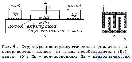
Soon, however, it became clear that the effect of the amplification of bulk AB by the drift electron flux in a piezoelectric semiconductor described above is difficult to use practically. The fact is that the electron mobility in good piezo-semiconductors (such as CdS, CdSe, etc.) is very small (~ 200 cm2 V-1 s-1), and in order to obtain the electron drift velocity on the order of the speed of sound (~ 3x105 cm s-1 ) it is necessary to apply a voltage of the order of several kilovolts. Because of the strong Joule overheating, such an amplifier can operate only in a pulsed mode. More promising in this regard are the EIA on surface waves. The structure of such an amplifier is shown in Fig. 4, a. With the help of an input lattice transducer (Fig. 4, b), sprayed onto the surface of the piezoelectric crystal Pe, the latter excites an acoustic wave. In some part of the surface of the piezocrystal in contact with the surface of the semiconductor wafer, in which a current flows from the source E. Consequently, in the area of the surface contact of the piezocrystal and the semiconductor, the acoustic wave will interact with the electron flow. It is in this area that the acoustic amplification of the signal occurs, which is then removed in the form of amplified alternating voltage from the output transducer operating in the reverse piezoelectric mode.
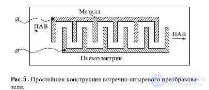
Let us consider the converter in more detail (Fig. 5).
In 1965, in their works, PM White and F. Voltmer [12] proposed to excite surfactants electrically with the help of a periodic structure of metal electrodes nested in a comb of metal on the surface of a piezoelectric - the so-called backward transducer (IDT). The period of the structure is equal to the wavelength, and an alternating voltage is applied to these combs with a period that is also equal to the wave period. This design allows you to convert the electrical signal to surfactant with high efficiency (loss of less than 1 dB).
The advantage of a surface-type EAC is that the materials of the piezoelectric and semiconductor may be different. The first of them should have high piezoelectric properties, the second should provide high electron mobility. As a semiconductor layer in such amplifiers, an n-type silicon monocrystal about 1 μm thick grown on an sapphire substrate by an epitaxial method is usually used. This material has a resistivity of the order of 100 Ohm • cm and the mobility of charge carriers up to 500 cm2 / (V • s). The length of the working part of the surface EIA is about 10 mm, width 1.25 mm, the power consumption of the direct current is about 0.7 W.

Comments
To leave a comment
Acoustoelectronics and acoustooptics
Terms: Acoustoelectronics and acoustooptics