Lecture
The purpose of the secondary power sources (VIP) is the conversion of the mains voltage into constant voltages of given nominal values necessary to ensure the operability of electronic circuits. There are two main structural schemes of the VIP: classical (mains transformer-rectifier-filter-stabilizer constant voltage) and pulse (rectifier mains voltage - high-frequency converter to pulse voltages of the required ratings - pulse voltage rectifier - smoothing filter - dc voltage stabilizer). The classical scheme, with its ease of implementation, has a significant drawback - a cumbersome mains transformer, so pulsed VIPs are widely used nowadays, which, despite a larger number of structural units, generally have smaller dimensions and weight because these parameters are incomparable in high-frequency transformers on ferrite cores Better than mains transformers with electrical steel cores. The block diagram of a classical VIP is presented in Figure 82. 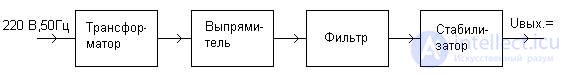
Fig.82
The structure of the classic VIP
Transformer - converts the mains voltage into alternating voltages required
mye for the formation of predetermined levels of constant output voltages. The choice of the type of magnetic circuit from standardized values is made according to the so-called gaba
power determined by a given power in the secondary windings (total
power load). For example, for full-wave rectifying Pgab. = 1.2 Rnag., The cross sections of the wires of the primary and secondary windings are also determined by the overall power, as well as the transformation ratio K = W1 / W2 and the allowable current density for copper wires, for example: I 2 = 1.1 Rgab. / Unagr. (effective current value of the secondary winding), I1 = I2 / K (effective current value in the primary winding).
Rectifier - converts an alternating voltage into a pulsating one, containing a constant component and an alternating voltage ripple. The half-wave rectifier circuit is shown in Figure 83. In the secondary power sources, this scheme is practically not used and has only theoretical interest. Timing diagrams are shown in Fig.84.
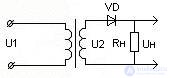
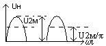
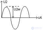
Fig.83 Fig.84
Simplest rectifier timing charts
Significantly improves the shape of the voltage curve at the load when the capacitor shunts it, this increases the constant voltage component and decreases the amplitude of the alternating ripple voltage, since the capacitor maintains the voltage at the load in the pause between the half-waves of the input voltage (Fig.8.8.86).
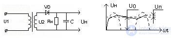
Fig.85 Fig.86
Resistive-capacitive load circuit Effect of capacitive load
full-wave rectifier
The most common scheme of a full-wave bridge rectifier , the circuit and voltage timing diagrams are shown in Fig. 87 and 88, respectively. 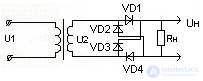

Fig.87 Fig.88
Bridge Rectifier Timing Charts
The filter plays the role of smoothing the pulsations at the rectifier output, usually
D - shaped LC filter, in the simplest case - single-link, implemented on the choke and the capacitor (Fig. 89). 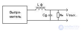
Fig.89.Single-block smoothing
LC filter
The stabilizer is designed to maintain a constant output voltage at a given range when the input voltage fluctuates (coming from the filter). Three basic stabilizer circuits are used: parametric, compensation, and pulse. The main parameter of the stabilizer is the stabilization factor, defined as:
Кст = (DUвх / Uвх) / (DУвых / Uвых)
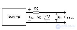
Here D - alternating increments of input and output voltages, respectively. The principle of operation of the parametric stabilizer is based on the property of the semiconductor element - the Zener diode to keep the voltage of a reversible breakdown (stabilization voltage) unchanged when oscillating within the known limits of the input voltage. The circuit and volt-ampere characteristic of the parametric stabilizer are shown in fig.90,91.
Fig. 90
Parametric stabilizer circuit
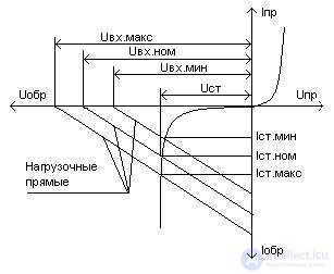
Fig.91
The working point is at the intersection of the characteristic of the Zener diode and the load line, the angle of inclination of which is determined by the value: R eqv = (Rb * Rh) / (Rb + Rh). Fluctuations in the input voltage cause changes in the current through the Zener diode relative to the nominal value, while the output voltage of the stabilizer remains almost unchanged. In this case, the load line moves parallel to itself. The ballast resistance Rb serves to limit the current through the zener diode,
which must be within acceptable limits at maximum deviations of the input voltage, the voltage on it is always equal to the difference between the input and output voltages. Using the Kirchhoff's law for loop currents, it can be shown that the stabilization factor will be: Fst = (Uout / Uin) * (Rb / Rst.din.), Where
Rsd.din = DUst / DIst- output dynamic resistance of the Zener diode, the value of which depends on the steepness of the falling branch of the characteristics of the Zener diode. For low-power zener diodes Rst.din is within 5 ... ..50 ohms. The stabilization factor of circuits of this type is low and is 10 ... .30 relative units, they are used mainly to limit stress levels, for example, to form reference voltages in comparators. Compensatory analog and pulse stabilizers, which incorporate an element controlled by a feedback circuit (usually a transistor), which compensate for the input voltage deviation, thereby maintaining the same voltage at the load, have more qualitative characteristics.
Analog compensation stabilizer monitors input voltage changes continuously. The principle of its operation is illustrated by the scheme shown in fig.92. 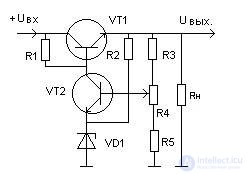
Fig.92
Compensation stabilizer
VT1 - adjustable transistor (plays the role of
a resistor connected in series with
load)
VT2 - regulating transistor (amplifier pos
current),
VD1 - Zener coarse installation Uout
To compensate for alternating deviations of the input voltage, the output voltage is set lower by 10–20% by selecting the Zener diode VD1 and the resistive divider R3, R4, R5 connected in parallel with the load, while the exact setting of the specified value is performed by the variable resistor R4. on an adjustable VT1 transistor, the voltage across the load is almost unchanged. Due to the amplifying properties of the VT2 transistor, very small voltage fluctuations on the load are monitored. The stabilizer has a high stabilization factor of -100 or more relative units, while in practical circuits, instead of VT2, an operational amplifier is used, as well as an integral design (IC of the K142 EN series). The drawback of the circuit is the continuous mode of operation of the adjustable transistor, which increases the power dissipated on it, and therefore it is necessary to use high-power transistors and heat sinks.
The output voltage regulator is largely free from this drawback, since the adjustable transistor operates in a lightweight mode, but it has a slightly higher ripple factor due to the need to filter the pulse sequence. In the general case, the block diagram of the DC voltage regulator is shown in Fig.93.
The impulse unit ensures the operation of the controlled element in the key mode, the characteristics of which are determined by the comparison unit. Two methods of control are used mainly: relay and pulse-width (PWM). In the first case, the pulses at the ER output have an amplitude equal to the input voltage at any given moment and regulation is provided by changing their duration. In the second case, the amplitude of the pulses is constant and their width changes according to the IB signals.
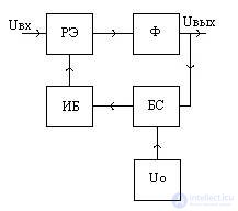
Fig.93
The structure of the pulse stabilizer.
RE - adjustable element, F - smoothing
filter, BS - output voltage comparison unit
with reference (setpoint), Uo is the source of reference
voltage, IB - pulse unit.
The principle of operation of the relay pulse stabilizer is illustrated by the scheme shown in Fig.94.
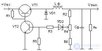
Fig.94
Relay Switching Stabilizer
Re in the circuit is represented by a VT1 transistor, connected according to a common emitter circuit, BS functions as a variable resistor R4 of the output voltage divider (R2, R4, R6). Zener diode VD2 serves as a source of reference voltage, IE is made on transistor VT2. Resistors R1, R3, R5 provide permissible modes of operation of transistors, the diode VD1 is necessary to protect VT1 from overvoltage due to emf. self-induction of the filter choke that occurs when the current through the inductance decreases (in the pause between pulses at the emitter VT1). The time diagram explaining the process of voltage regulation on the load with deviations of the input voltage relative to the nominal value is shown in Fig.95.
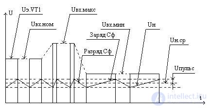
Fig.95
The process of relay regulation
in pulse
stabilizer.
The rise of Un during the pulse Ue.VT1 is limited by the moment of equality of the voltage taken from the slider R4 to the sum of the breakdown voltage of the zener diode and the threshold opening voltage of the transistor VT2. In the pause between pulses, the filter capacitor discharges to the load resistance until the moment when U equals the Zener diode breakdown voltage. The voltage difference between the operation of the sravneiya block (hysteresis) determines the magnitude of the ripple relative to the average voltage value at the load. The advantage of the above scheme is the relative simplicity at an acceptable level of the ripple coefficient, a pulse stabilizer with PWM control circuit is more complex than the circuit, but it has the best quality indicators of the output voltage. The block diagram of the pulse VIP is shown in Fig.96. 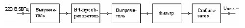
Fig.96. Switching power supply
A new element here is a high-frequency DC-to-pulse converter. Transformer cascades controlled by a master pulse generator or pulse oscillators with self-excitation are used as such a converter. The frequency conversion is usually in the range of 30 - 50 kHz. As an example, Fig.97 shows a simplified scheme of a push-pull blocking generator (Roer's circuit), which is a multivibrator with electromagnetic coupling of the collector windings of a high-frequency transformer with positive feedback windings connected to the bases of transistors. The voltages on the base windings are proportional to the rate of change of the magnetic flux in the core of the high-frequency transformer T (dФ / dt). The windings are turned on in such a way that with a positive derivative on one of them arises
unlocking one of the transistors, voltage, and the other voltage of opposite polarity, locking the transistor of the other “arm” of the circuit. This state is maintained until the magnetic flux reaches the maximum value determined by the amperages of the corresponding collector winding and the magnitude of the collector power Ек, the transistor is fully open and its resistance is low. The dF / dt derivative and the unlocking voltage become zero and the transistor starts to close, which leads to a decrease in the magnetic flux, a change in the sign of the derivative and the appearance of a locking voltage on the transistor of the “shoulder” and, accordingly, the unlocking voltage at the base of the other transistor. Next, there is an increase in the magnetic flux of the opposite direction, initiated by the second “shoulder” and the processes are repeated. It should be noted that the pulse duration of the collector current and, consequently, the voltage transformed into the secondary winding (Uout.) Depends not only on the rise time of the magnetic flux (inductance of the collector winding), but also on the inertia of the transistor, i.e. from the time it is turned off. Timing diagrams at the main points of the scheme are shown in Fig.98. 
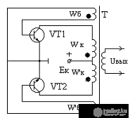
Fig.97 Fig.98
Two-stroke Time Generator
Roera chart
The remaining blocks of the above block diagram of the pulse VIP are not fundamentally different from those for the VIP, made according to the classical scheme.
In a general sense, a pulse technique should be understood as a set of calculation methods and technical means, allowing to realize devices for logical processing of pulse signals. A rectangular pulse signal is usually called a jump change in currents and (or) voltages, while these parameters can take only two values: high and low (logical 0 or 1). In the so-called positive logic, logical 1 corresponds to high level, low - logical 0, in negative logic, it is the other way round. Figure 99 shows the timing diagram of a rectangular pulse with its characterizing parameters.
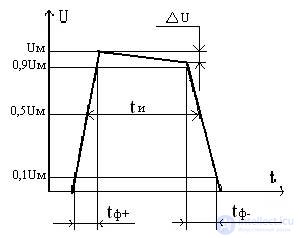
Pic.99
Pulse parameters
Um - the amplitude of the pulse,
g = DU / Um - relative blockage
the tops of the pulse
tand - the pulse duration
tf + - the leading edge of the pulse,
tf- - the trailing edge of the pulse.
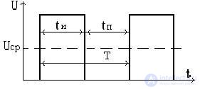
The duration of the pulse fronts represent the time during which the pulse voltage changes from 10% to 90% of the maximum value — the leading front, or from 90% to 10% - the falling edge. The sequence of pulse signals is shown in Figure 100 and, apart from the parameters of a single pulse, is characterized by a number of additional characteristics such as the period (time interval between identical phases of two neighboring pulses), duty cycle (ratio of period to pulse duration), average voltage (constant component) of the pulse sequence , pause (time interval between the falling and leading edges of two adjacent pulses).
Pic.100
Impulse sequence
tп - pause
Duty ratio can be expressed as: Q = T / t and = (T and + tp) / t and = 1 + tp / t and, with a duty cycle equal to two (t and = t), the sequence of pulses is called "meander". The average voltage of a pulse sequence is: 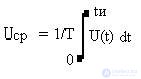 , for U (t) = Um = Const we get: Ucr = Um * ti / T
The above pulse signal belongs to the class of video pulses, the most common in the pulse devices of IIT. Other classes of pulse signals: radio pulses, special-shaped pulses are not considered here. The basis of the construction of logical devices of any degree of complexity are the so-called basic logic elements that perform the simplest logical operations, they are present in almost all modern series of digital integrated circuits. Так основой широко распространенной серии ИС транзисторно-транзисторной логики (ТТЛ-серии: К155 и усовершенствованные модификации К533, К555,К1533 и др.) является ключевой элемент (ключ) на биполярном транзисторе , выполняющий операцию логического отрицания. Используется также название ключа- инвертор.
Схема транзисторного ключа приведена на рис.101. Характерной особенностью схемы является работа транзистора либо в режиме “закрыт” – рабочая точка на выходных характеристиках транзистора располагается на границе области отсечки (логический 0 по коллекторному току), либо в режиме “ открыт ” – рабочая точка располагается на границе области насыщения (логическая 1 по коллекторному току). Кроме того, из-за инерционных свойств транзистора переход рабочей точки из одного состояния в другое происходит не мгновенно, поэтому необходимо учитывать переходный процесс переключения, влияющий на параметры выходного импульса коллекторного тока.
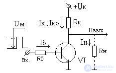
Рис.101
Схема транзисторного ключа
Физически логические переменные Х и Y представлены уровнями напряжений входного и выходного сигналов соответственно. Условное графическое изображение инвертора показано на рис.102.

Рис.102
УГО инвертора
В состоянии насыщения транзистор как бы “стянут” в точку, грубой аналогией этого состояния может служить замкнутый механический тумблер. При этом в идеальном случае должно быть Uвых = 0 (логический 0 ),однако, реально Uвых равно напряжению насыщения транзистора (около 0,5В для Si – транзисторов), это напряжение называют остаточным параметром , характеризующим неидеальные свойства транзисторного ключа в указанном режиме. В режиме насыщения ток коллектора максимален , ограничен только сопротивлением коллекторной нагрузки Rк, обозначается символом Iк.н (ток коллектора насыщения) и равен:
Iк.н = (Uк – Uнас.)/Rк » Uк/Rк, поскольку Uнас.« Uк
Для поддержания коллекторного тока насыщения очевидно необходимо создать ток в базе транзистора теоретически величиной не менее:
Iб.н = Iк.н/h21Э – ток базы насыщения,h21Э- коэффициент передачи базового тока в коллектор для схемы с общим эмиттером.
Практически из – за технологического разброса h21Э, а также его нестабильности в температурном диапазоне реальный базовый ток должен быть больше теоретического значения, величина реального тока базы равна:
Iб.реал. = (Uм-Uбэ)/Rб » Uм/Rб, поскольку напряжение на открытом базо-эмиттерном переходе Uбэ«Uм.
Отношение: Iб.реал./ Iб.н = S называют коэффициентом насыщения (практически его величина лежит в пределах 5-10 относительных единиц).
В состоянии отсечки сопротивление между коллектором и эмиттером транзистора велико, грубой аналогией в этом случае является разомкнутый механический тумблер. При этом напряжение на выходе в идеальном случае должно быть равно напряжению коллекторного питания (если сопротивление нагрузки ключа бесконечно велико) и трактуется как логическая 1. Однако, из-за наличия теплового тока коллектора образуется напряжение на коллекторном резисторе и реальное напряжение на выходе будет равно:
Uвых= Uк – Iко*Rк (Rн = ?), т.е. несколько меньше (на единицы милливольт) идеального. Напряжение Iко*Rк, также называется остаточным параметром в режиме отсечки и характеризует неидеальность ключа в этом режиме. Кроме того, указанный режим
накладывает ограничения на предельную величину резистора, ограничивающего базовый ток. Поскольку тепловой коллекторный ток создает напряжение на этом резисторе, причём его полярность является отпирающей для транзистора, то при слишком большой величине Rб транзистор из состояния отсечки может перейти в активный режим, т.е. произойдёт несанкционированное срабатывание ключа (низкий уровень напряжения логической 1 или вообще переход транзистора в открытое состояние). Опасность несанкционированного срабатывания резко возрастает, если ключ работает в широком температурном диапазоне, поскольку тепловой ток коллектора удваивается на каждые 10оС повышения температуры окружающей среды. Очевидно, что величина Rб должна быть ограничена сверху в соответствии с условием:
Rб ? Uбэ.пор./Iко.макс.,где Uбэ.пор.- напряжение отпирания транзистора по базе, Iко.макс.- максимальное значение теплового тока для данного типа транзистора и заданных условий внешней среды.
Переходный процесс переключения транзистора между указанными состояниями исследуется с помощью так называемого метода заряда в базе транзистора. Суть метода заключается в следующем - скорость изменения заряда в базе при переключениях ключа можно записать как:
dQ/dt = Iб – Q/t , где Q – заряд, Iб – установившееся значение тока базы, t -постоянная времени транзистора (пропорциональна времени жизни неосновных носителей заряда в базе), после очевидных преобразований получим:
t* dQ/dt +Q = Iб*t – неоднородное дифференциальное уравнение первого порядка, аналогичное уравнениям, описывающим поведение RC – цепей с одной реактивностью в переходном процессе, решение таких уравнений рассматривается в курсе теоретических основ электротехники и выглядит следующим образом:
Q(t) = Q(?) - [Q(?) – Q(0) ]*е-t/t ,
здесь Q(?) и Q(0)- граничные условия (установившиеся значения заряда через бесконечно большой промежуток времени и в начальный момент соответственно). Вид функции представлен на рис.103.
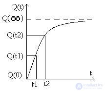
Рис.103
Экспоненциальная зависимость изменения
заряда в базе при включении транзисторного
ключа
Практический интерес представляет также интервал времени в течение которого заряд изменяется в определённых пределах, например для рис.103, в пределах от Q(t1) до Q(t2) из общего решения можно найти моменты времени t1, t2 и их разность:
Dt = t2 – t1 = t*ln{Q(?)-Q(t1)}/ {Q(?)-Q(t2)}
Временные диаграммы, поясняющие процесс переключения транзисторного ключа при подаче на его базу прямоугольного импульса тока и влияние переходного процесса на форму и параметры выходного (коллекторного) импульса тока приведены на рис.104.Обозначения на рис104:
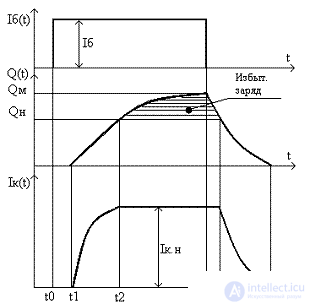
Рис.104
Временная диаграмма переходного
процесса в транзисторном ключе.
tзад. = t1-t0 –время заряда базо-коллекторной
ёмкости, приблизительно 0,25 t
tф+ = t2 –t1 - передний фронт коллектоного
импульса тока,
tрас. = t4 –t3- время рассасывания избыточного
заряда базы,
tф- = t5 – t4 –задний фронт коллекторного им-
пульса тока,
Dt = t3 – t2 – время накопления избыточного
заряда в базе (не влияющего на величину кол-
лекторного тока).
Пользуясь приведенными выше соотношениями, можно определить временные параметры импульса коллекторного тока, так для длительности переднего фронта получим:
Q(?) = Qм, Q(t1) = 0, Q(t2) = Qн - граничные условия рассматриваемой фазы импульса,
tф+ = t*ln{Q(м)-0}/ {Q(м)-Q(н)} = t*lnt*Iб/( t*Iб - t*Iбн) =t*ln 1/(1- Iбн/ Iб)= t*ln S/(S-1)
Применим разложение функции натурального логарифма в степенной ряд вида:
lnx »(x-1)/x +…, где х = S/(S-1), получим: tф+ » t/S
Из полученного выражения следует, что для уменьшения длительности переднего фронта необходимо увеличивать степень насыщения транзистора на этапе включения.
Таким образом, время включения транзистора при подаче отпирающего импульса тока в базу составит:
tвкл.= tзад.+ tф+= 0,25t+t/S
По изложенной методике найдем время рассасывания избыточного заряда в базе:
tрас. = t*ln {Q(t5) – Q(t3)}/ {Q(t5) – Q(t4)} = t*ln(0-t*Iб)/(0-t*Iбн)»t{1 – (1/S)}
В данном случае необходимо уменьшать насыщение транзистора, чтобы ускорить процесс его выключения , т.е. для улучшения параметров импульсов выходного коллекторного тока необходимо удовлетворить противоречивые требования относительно коэффициента насыщения транзистора.
Длительность заднего фронта выходного импульса найдем , предполагая, что его формирование закончилось при снижении величины заряда в базе до уровня 0,1Qн,тогда:
tф- = t*ln {Q(t5) – Q(t4)}/ {Q(t5) –0,1Q(t4)} = t*ln(0-t*Iбн)/(0-0,1t*Iбн) = 2,3t
Таким образом, время выключения транзистора составит: tвыкл. = tрас.+ tф-»t{3,3-(1/S)}.
Обычно время задержки срабатывания определяется как: tз.ср. = 0,5(tвкл.+tвыкл.)
Известны методы ускорения переходных процессов транзисторного ключа, основные из них приведены ниже.
Метод форсирующего конденсатора основан на свойстве конденсатора сохранять неизменным напряжение на нём в момент поступления переднего фронта входного импульса, т.е. фактически в этот момент его реактивное сопротивление равно нулю (первый закон коммутации теории переходных процессов в RC-цепях). Схема включения форсирующего конденсатора приведена на рис.105. 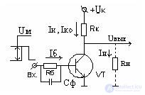
Fig. 105
Включение форсирующего конденсатора Сф
Временные диаграммы, поясняющие принцип работы форсирующего конденсатора показаны на рис.106. 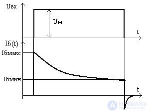
Рис.106
Ток базы ключа при наличии
форсирующего конденсатора
В момент включения ток базы достигает максимальной величины –Iбмакс=Uм/Rбэ,где Rбэ- входное сопротивление транзистора, тем самым обеспечивается высокое значение коэффициента насыщения и минимальная длительность переднего фронта импульса коллекторного тока. По мере заряда конденсатора ток базы уменьшается и в конце входного импульса достигает минимальной величины Iбмин.=Uм/(Rб+Rбэ),обеспечивающей S=1.
Метод введения нелинейной отрицательной обратной связи с использованием диода Шоттки также обеспечивает разное насыщение транзистора в процессе его коммутации аналогично предыдущему случаю, однако технологически проще реализуем в интегральном исполнении. Особенностью диода Шоттки является малый порог срабатывания и высокое быстродействие, благодаря чему отрицательная обратная связь срабатывает раньше чем транзистор ключа войдет в насыщение. Схема ключа с диодом Шоттки представлена на рис.107. 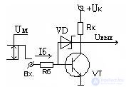
Fig. 107
Нелинейная обратная связь с диодом
Шоттки
Падение напряжения на диоде Шоттки обеспечивает положительный потенциал коллектора относительно базы, предотвращая тем самым смещение коллекторно-базового перехода в прямом направлении и накопление избыточного заряда в базе. В современной схемотехнике ИС серии ТТЛ диод Шоттки интегрирован с транзистором (серии ИС ТТЛШ).
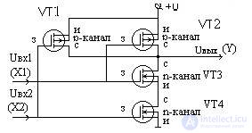
Инвертор (ключ) на полевых транзисторах является основой популярной серии ИС-КМОП (К561,564).Ключ выполнен на двух полевых транзисторах с дополнительной симметрией ( К- дополнительный),т.е. транзисторы имеют каналы различного типа проводимости. На рис.108 приведена схема такого ключа на полевых транзисторах с индуцируемыми каналами “p” и “n” типа.
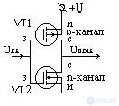
Рис.108
Ключ на полевых транзисторах с дополнительной
симметрией
Переключение ключа происходит , когда входное напряжение превышает по модулю порог срабатывания транзисторов. При этом Uпор.vт1 » -0,5U, Uпор.vт2 » +0,5U, таким образом при Uвх = 0 (логический ноль): VТ2 – закрыт, VТ1 – открыт, поскольку на его затворе действует потенциал равный минус U, на выходе формируется высокий уровень, примерно равный напряжению питания +U (логическая единица). При Uвх » +U (по входу ключ управляется выходным напряжением аналогичного элемента), состояние транзисторов противоположно предыдущему и на выходе напряжение оказывается близким к нулю (логический 0).Таким образом выполняется операция логического отрицания, в статическом состоянии ток потребления практически отсутствует, т.к.один из транзисторов всегда закрыт. При переключениях появляется входной ток, связанный с перезарядом подзатворных емкостей, величина этого тока тем больше, чем выше частота входного сигнала. Кроме того, наличие этих емкостей ограничивает частотный диапазон работы ключа и , следовательно, КМОП серии ИС, что сужает диапазон её применения.
На основе рассмотренных ключей строятся так называемые базовые элементы основных серий ИС: И-НЕ (штрих Шеффера), ИЛИ-НЕ (стрелка Пирса), на которых возможна реализация сложных логических устройств с наименьшими затратами аппаратных средств.
Базовый элемент И-НЕ серии ИС ТТЛ имеет условное графическое обозначение, показанное на рис.109 , выполняет логическую операцию , таблица истинности приведена ниже. 
Рис.109
Truth table
УГО логической
операции
штрих Шеффера
The principle of operation and the technical implementation of the specified element are shown in Figure 110. The basis of the circuit is a multi-emitter transistor VT1, performing a conjunction operation (AND), in fact it is an integrated set of diodes by the number of inputs -2 and outputs -1. The operation is NOT implemented by Vt2, Vt3, Vt4 transistors with simultaneous amplification of the output signal. Diodes VД1, VД2 are necessary to increase the thresholds of the operation of transistors VT2 and VT3 in order to secure them safely at low levels of input voltages. Resistors R1? R4 provide permissible modes of operation of transistors for the base and collector currents of transistors. A characteristic feature of TTL circuits is + 5V supply voltage.
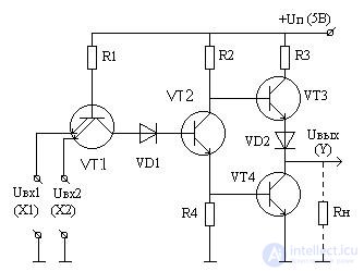
Pic.110
The scheme of the basic element and NOT
Ttl
We introduce the notation of the physical levels of logical 1 and 0 as E1 and E0, respectively.
The operation of the base element is as follows:
Uin1 = Uin2 = E0 - emitter outputs VT1 are connected to a common point through internal resistances of input sources, the basic emitter junctions are open and shunt the collector-base transition VT1, the base current VT2 is zero and the transistors VT2 and VT4 are closed, in this case the transistor
VT3 is unlocked by the base current along the circuit: UP-R2- base-emitter junction VT3-
VД2-Rн-common point, a high voltage level is formed at the output:
Е1 "Uп * Rн / (R3 + Rн) - logical 1;
Uin1 = E1, Uin2 = E0 or Uin1 = E0, Uin2 = E1 - the state of the circuit does not change, since the collector-base transition VT1 is shunted from the open basic-emitter junction, the output is logical 1;
Uin1 = Uin2 = E1 - both base-emitter transitions VT1 are closed by high blocking voltages, the collector-base transition of the VT1 transistor opens and its collector current opens the VT2 transistor along the circuit: Up-R1-collector-base transition VT1-VD1-base VT2, emitter VT2 current creates a voltage across the resistor R4, unlocking the VT4 transistor, thus the output terminal is connected to a common point through a low resistance between the collector and the open VT4 emitter and a low voltage E0 (logical zero) is generated at the output.
Thus, the above scheme implements the truth table of the logical operation Scheffer stroke. A typical representative of the considered basic logic element is a chip series TTL - K555LA3, containing 4 two-input elements AND-NOT, UGO of this chip is shown in Figure 1111. 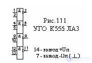
The main parameters and characteristics of the basic logic element TTL :
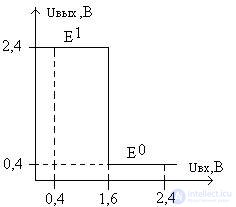
Pic.112
Transfer characteristic
basic TTL element
1.6 V - threshold voltage
actuation
For the state Uin = E0 and Uout = E1, a false triggering of the element is possible if the interference voltage with respect to the “ground” bus is equal to: Uppom. ? 1.6 - 0.4 = 1.2V.
For the state Uin = E1 and Uout = E0, a false positive is possible if the voltage of the interference with respect to the bus “power” is equal in absolute terms to Upom.pit.? 2.4 - 1.6 = 0.8V. Practically, taking into account the influence of the ambient temperature, the permissible interference is no more than 0.6V.
the power consumed by the basic logic element is relatively large and amounts to about 20 mW.
It should be noted that the elements of TTL are sensitive to the magnitude of the internal resistance of the input source (Ri), indeed, if Ri? 1Kom, then in the state Uin = E0, the voltage drop across it from the input current may exceed the threshold voltage, which will lead to unauthorized tripping.
The base logic element AND is NOT the IC CMOS series .
The basis of this series of ICs is the previously discussed key on field-effect transistors with additional symmetry, UGO, a logical equation, a truth table similar to those given for the AND-NOT TTL element.
The power supply voltage of the IC of this series differs in a wide range of 3 ... 15 V, the power consumption in static mode does not exceed 0.1 mW, the input resistance is very large (> 1 Megohm), thanks to which CMOS ICs are widely used in circuit design in cases where no increased requirements are made to speed. The speed of a CMOS logic element is in the range of 100–200 nanoseconds and is determined by the properties of the key element discussed above. The principle of operation of the basic element is illustrated by the scheme shown in Figure 113.
Pic.113
CMOS logic element
Sheffer's stroke
The operation of the base element is as follows:
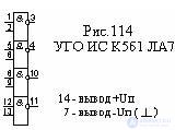
The basic element of the IC CMOS series has a high noise immunity: Um.pit "Upom.zem" 0,5 Upit. Due to the high input resistances, the branching factor “n” can reach 100 units. A typical example of manufactured ICs of the considered type is the chip shown in Figure 114.
The basic logic element of ECL series ECL ( emitter-coupled logic) .
Distinctive features of this series are:
The diagram of the basic logic element (WEL) in this series of the IC shown in Figure 115 performs two logical operations: 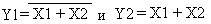
The truth table is as follows:
Pic.115
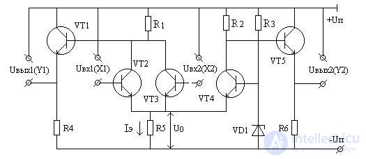
Basic element ECL 2 OR, 2, OR NOT
Transistors VT1 and VT5 operate in the mode of emitter followers, providing amplification of output signals in power. Transistors VT2, VT3 are input, their bases are supplied with voltages corresponding to logic levels E1 and E0, measured relative to a common point and, therefore, having a negative polarity. The VT4 transistor is a reference, setting the switching mode of the input transistors, the potential of its base (Uо) is fixed constant relative to the + Uп bus in this case using the Zener diode VD1 (other methods are possible). The emitters of the input and reference transistors are interconnected (hence the name ECL) and connected to a common negative feedback resistor for emitter current R5. All transistors have the same parameters, since they are made in a single technological process. Resistors R1, R2 are collector loads, resistor R3 - sets the current mode of the Zener diode, resistors R4, R6 - emitter followers load.
The principle of operation of the BLE is based on switching the emitter current of the reference transistor to one or both input transistors depending on the combination of input signals, in the latter case the current of the reference transistor is divided in half between the input transistors due to the symmetry of the circuit.
Consider the operation of an element with combinations of input and output signals in accordance with the truth table. According to the first row of the table, both input signals have a low logic level, i.e. Uin1 = Uin2 = E0 - transistors VT2, VT3 are closed, because the potentials of their bases relative to the bus –Up is less than the negative feedback voltage Uо by the value of DUBe. This is explained by the fact that the logical elements of one series are connected to each other, and for the combination of input signals under consideration, it can be assumed that the base VT2, VT3 receives voltage from the output of another BLA that is in the state of logical zero, i.e. in this case, similar to the existing resistor R6. The reference transistor VT4 is open, its mode of operation is close to the emitter follower, since the ratio R2 R R5 is circuit-implemented and the reference voltage (Uо) is almost completely repeated on the OOS R5 resistor. Since VT4 is open, the potentials of its collector and VT5 base are at a low level relative to the –Un bus. Consequently, the voltage across the bus –Un on the resistor R6 is also small, i.e. less Uo: DUbe = Uo - UR6. Then the output voltage, measured relative to the common point (+ Up), equal to the voltage drop between the collector and the emitter VT5, will be high in magnitude: | Uout2 | = | Up | - | UR6 | and low, taking into account its sign ("-1.5 V), this value in the ECL IS series corresponds to the logical zero Y2 = 0 (direct output of the BLE). In turn, the high potential relative to the –Un bus of the combined collectors of closed VT2, VT3 will be repeated on the emitter load VT1 - resistor R4 and, therefore, Uout1 will be small in modulus and large given the sign ("-0.9V), i.e. . correspond to logical 1: Y1 = 1 (inverse output).
For combinations of input signals: Uin 1 = E1, Uin 2 = E0 ; Uin1 = E0, Uin2 = E1 ;
Uin1 = E1, Uin2 = E1 , implementing 2 th , 3 th and 4 th lines of the truth table, respectively, occurs, as mentioned above, switching the current of the reference transistor to an open input transistor. For example, for the combination Uin1 = E1, Uin2 = E0, the VT2 transistor is opened with a high voltage level relative to the –Un bus coming from the analogue of the R4 resistor of the previous element, which is in the Y1 = 1 state. The circuitry ensures the ratio: Uin1 = Uo + Dube, this voltage is almost completely repeats on the feedback resistor R5, as a result, the voltage on the base of the reference transistor becomes negative and it closes: DUBe.BT4 = U0 - U-Dube = -DUe.
Thus, the current of the reference transistor switches to the input transistor VT2,
the potential of the collector of VT2 (and the base of VT1) relative to the –Un bus decreases, the low potential of the base of VT1 is repeated almost without change on resistor R5.
Thus, at the output of VT1, a high-modulated and low, taking into account the sign, voltage Uout1 ”-1.5V is formed, interpreted as a logical zero (E0) at the inverse output, it is likewise easy to see that at the forward output Uout2” -0.9V, ie, the logical unit (E1). The processes occurring in the circuit for the remaining combinations of input signals do not fundamentally differ from those discussed above (in the last combination, the current of the reference transistor switches to both input transistors and is divided between them in half). It should be noted that due to the high amplifying properties of transistors, the voltage of their switching is very small: DUBe ”50mV, moreover, it is obvious that the following relationship should be satisfied: Uo = (Е1 + Е0) / 2 = - (0.9 +1.5) / 2 = -1.2V. The switching process is explained by the transfer characteristics shown in Fig.116 for direct and inverse outputs.
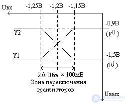
Pic.116
Transfer characteristic
basic logic element ECL
2 OR, 2, OR NOT
The advantage of ECL ECL series is high speed - ts.sr. ? 1 ... 2nS, due to the fact that the transistors in the open state operate without saturation due to deep negative feedback and a small amount of unlocking voltage, due to which the base charge resorption time is short and, therefore, the off time of the input transistors is short. The turn-on time is also short due to the regenerative switching mode associated with the OS and the short recharge time of the input capacitors of the transistors through relatively small resistors (R1 = R2 = 200 ... 300 Ohms). The disadvantages of ECL EC include: high power consumption associated with the operation of emitter repeaters in the active mode (? 50 mW) and low noise immunity due to low levels of switching voltages. For these reasons, the ECL series is of limited use.
The ECL series of ICs include К1500, К1590, as a practical example in Fig.117 the conditional graphic image of the element К1590 ЛМ105 is given.
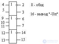
Fig.117
Basic element of ESL K1590LM105
2 (2IL, 2IL - NOT), 3IL, 3IL - NOT
Comparative table of basic elements
Type of |
| E1 | Rpotr. | tz.s.r. | Coeff. | Interference | U. |
Ttl | 0.2 - 0.4 | 2.4 - 4 | ? 20 | 5 ... 20 | ?ten | 0.8 ... 1.1 | +5 |
CMOS | 0.2 - 0.4 | »0.9Un. | ? 0,1 | 200 200 | up to 200 | »0.5U. | + 3 ... 15 |
ECL | - 1.5 | - 0.9 | 20 ... 50 | 1 ... 3 | ?ten | ? 0.3 | - five |

Comments
To leave a comment
ENGINEERING PSYCHOLOGY AND ERGONOMICS
Terms: ENGINEERING PSYCHOLOGY AND ERGONOMICS